


GM47/GM48 INTEGRATOR’S MANUAL
26
LZT 123 7263 R1C
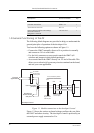
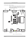
1.3 General Functioning of the Kit
The following block diagrams are provided to help you understand the
general principles of operation of the developer’s kit.
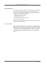
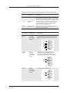
You have the following options as shown in Figure 1.1:
• Connect the GM47 internally, direct to J4 or position it externally
and connect to J10 via a flat cable.
• Use the kit’s connectors to access and control the GM47 (all
switches and jumpers in their default positions).
• Access and control the GM47 directly via J12 and a flat cable. This
allows you to selectively bypass any circuits contained on the board,
and test your own application.
Figure 1.1 Module connections to the developer’s board
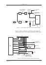
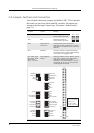
Figure 1.2 shows the various on-board voltages and how they are fed to
the GM47 and other circuitry. The developer’s board is powered by an
external power supply connected to Vcc.
Cable with connector/cable serial 9-9 PIN DB9(M)-DB9(F) 1
Portable handsfree 2002-1-24 1
Quad band antenna RG174 1
Data carrier/CD-ROM containing:
Software Manual;
Integrator’s Manual
LZY 213 1319 1
Description Product Number Qty
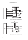
External
Application
J4J10
J11
J12
Developer's
board circuits
and ports
User selectable
jumpers
Pin headers
60 pins female
1.27mm pitch
Pin header
60 pins male
2.54mm pitch
Pin header
60 pins male
1.27mm pitch
GM47
Developer's board
fit direct to J4
alternate flat cable to J10
Pins connected in parallel