


GM47/GM48 INTEGRATOR’S MANUAL
54
LZT 123 7263 R1C
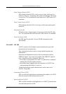
PCM Timing Diagrams
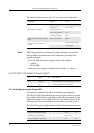
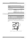
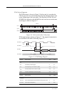
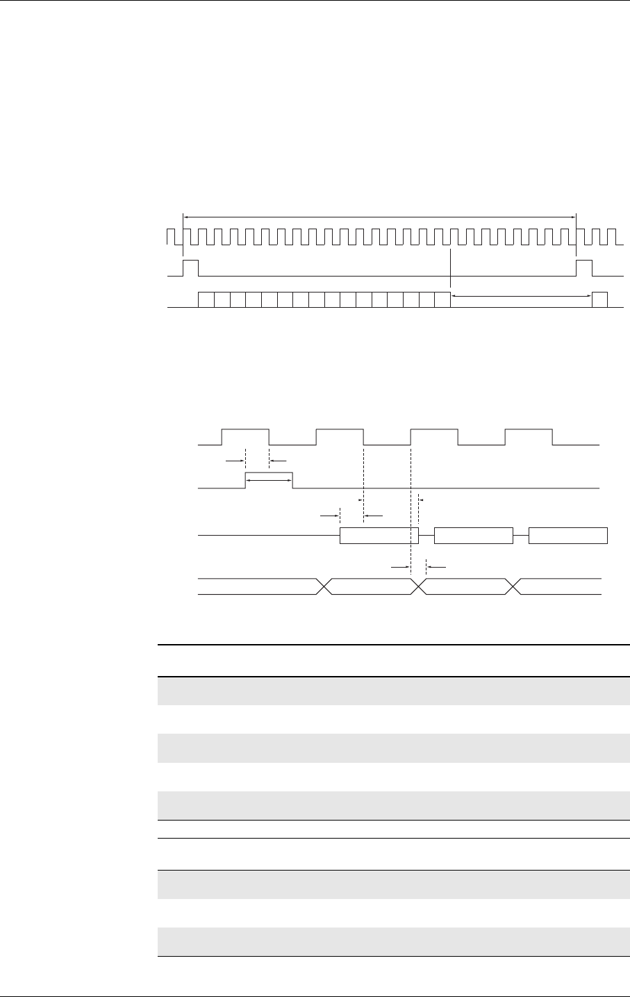
The PCM timing is shown in Figure 2.6 below and it is seen that the
CPU has 45µs to serve an interrupt and setup data channels. Data is sent
on the falling edge of the sync pulse. The data bits in PCMULD and
PCMDLD are aligned so that the MSB in each word occurs on the same
clock edge as shown in Figure 2.7.
Figure 2.6 16-bit word within 24-bit frame
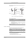
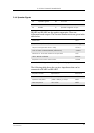
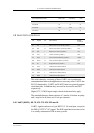
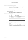
PCM signal timing is shown in Figure 2.7. The signals characteristics
are described in the tables following Figure 2.7.
Figure 2.7 PCM Timing Diagram
Clk
Sync
Data
45 µs
125 µs
PCMCLK
PCMSYN
PCMIN
PCMOUT
XMSB D14 D13
MSB
D14 D13
t
PSS
t
PSH
t
DSL
t
DSH
t
PDLP
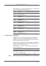
Name Description Typ. Unit
t
PSS
PCMSYN (setup) to PCMCLK (fall) 2.5 µs
t
PSH
PCMSYN pulse length 5 µs
t
DSL
PCMI (setup) to PCMCLK (fall) 2.5 µs
t
DSH
PCMI (hold) from PCMCLK (fall) 2.5 µs
t
PDLP
PCMO valid from PCMCLK (rise) 2.5 µs
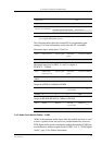
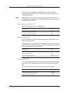
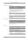
Name Description Typ. Unit
F
PCMCLK
PCM clock frequency 200 kHz
T
PCMCLK
PCM clock period with 50/50 mark space ratio 5 µs
F
PCMSYN
PCM sync frequency 8 kHz