


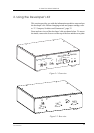


GM47/GM48 INTEGRATOR’S MANUAL
36
LZT 123 7263 R1C
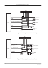
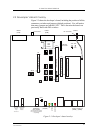
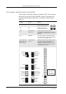
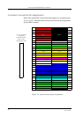
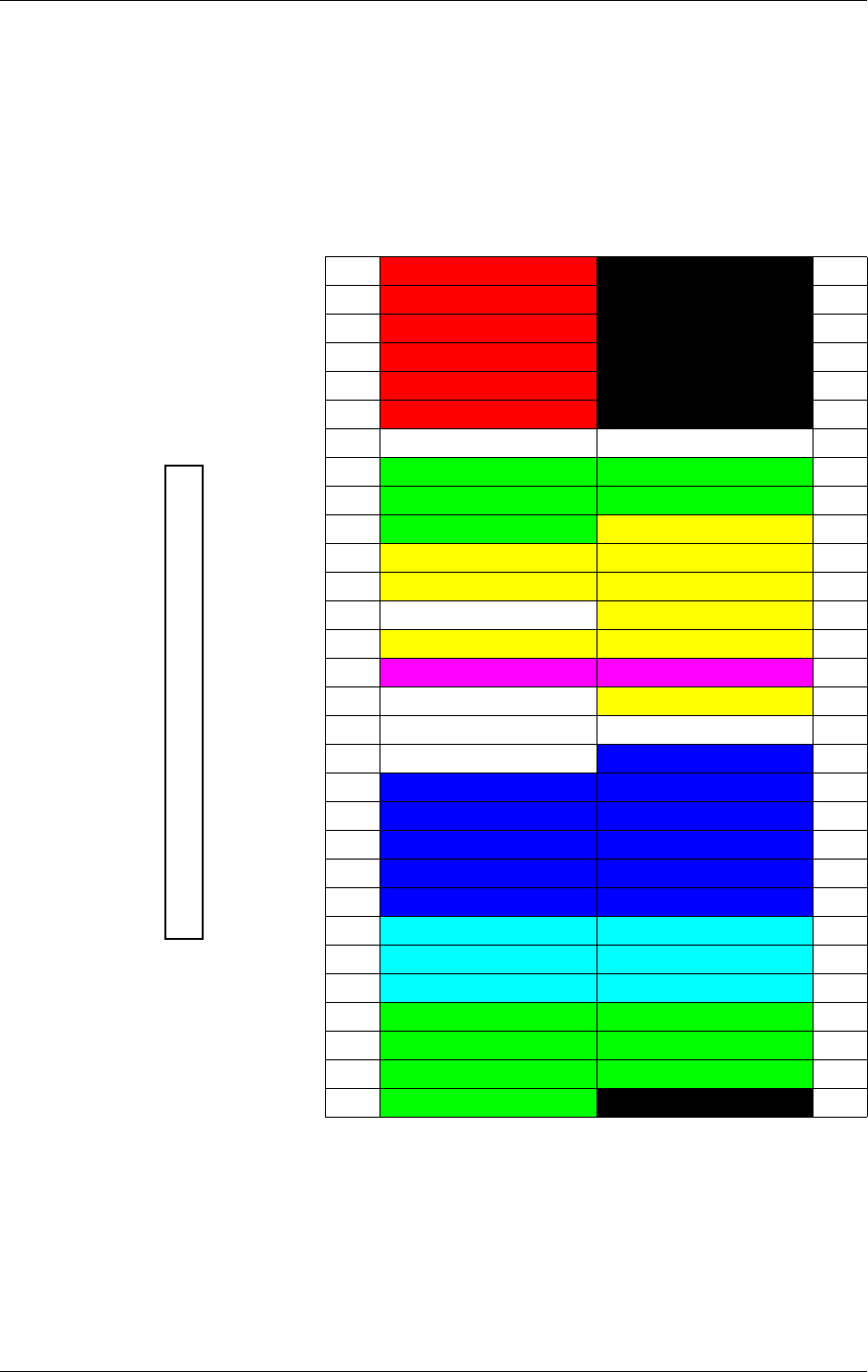
2.4 System Connector Pin Assignments
Refer to the table below when monitoring signals on, or connecting to,
J10, J11 or J12. The table shows the system-connector pin assignments
for the GM47 module.
Figure 2.4 System connector pin assignments
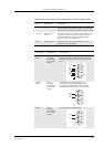
1 VCC DGND 2
3 VCC DGND 4
5 VCC DGND 6
7 VCC DGND 8
9 VCC DGND 10
11 VCC DGND 12
13 Reserved for future use ON/OFF 14
15 SIMVCC SIMPRESENCE 16
17 SIMRST SIMDAT 18
19 SIMCLK DAC 20
21 IO1 IO2 22
23 IO3 IO4 24
25 VRTC ADC1 26
27 ADC2 ADC3 28
29 SDA SCL 30
31 BUZZER OUT5 32
33 LED VIO 34
35 TX_ON RI 36
37 DTR DCD 38
39 RTS CTS 40
41 TD (DTMS) RD (DFMS) 42
43 TD3 (TX3) RD3 (RX3) 44
45 TD2 (CTMS) RD2 (CFMS) 46
47 PCMULD PCMDLD 48
49 PCMOUT PCMIN 50
51 PCMSYNC PCMCLK 52
53 MICP MICN 54
55 BEARP BEARN 56
57 AFMS SERVICE 58
59 ATMS AGND 60
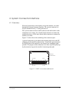
12
59 60
J10, J11 & J12 pin
numbering
viewed from the
front of the
developer’s box