


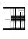
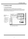
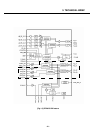
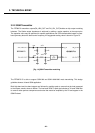
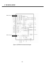

A generic, high-level functional block diagram of U250/KU250 is shown in Figure 1-1. One antenna
collects base station forward link signals and radiates handset reverse link signals. The antenna
connects with receive and transmit paths through a FEM(Front End Module).
The UMTS receive path each include a LNA, a RF band-pass filter, and a downconverter that translate
the signal directly from RF-to-baseband using radioOne ZIF technique. The RFIC Rx analog baseband
outputs, for the receive chains, connect to the MSM IC. The UMTS and GSM Rx baseband outputs
share the same inputs to the MSM IC.
For the transmit chains, the RTR6275 IC directly translates the Tx baseband signals (from the MSM
device) to an RF signal using an internal LO generated by integrated on-chip PLL and VCO. The
RTR6275 IC outputs deliver fairly high-level RF signals that are first filtered by Tx SAWs and then
amplified by their respective UMTS PA. The high- and low-band UMTS RF transmit signals emerge
from the RTR6275 transceiver.
In the GSM receive paths, the received RF signals are applied through their band-pass filters and
down-converted directly to baseband in the RTR6275 transceiver IC. These baseband outputs are
shared with the UMTS receiver and routed to the MSM IC for further signal processing.
The GSM transmit paths employ one stage of up-conversion and, in order to improve efficiency.
1. The on-chip quadrature up-converter translates the GMSK-modulated signal to a constant envelope
phase signal at RF;
2. The amplitude-modulated (AM) component is applied to the ramping control pin of power amplifier
from a DAC within the MSM
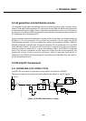
U250/KU250 power supply voltages are managed and regulated by the PM6650 Power Management
IC. This versatile device integrates all wireless handset power management, general housekeeping,
and user interface support functions into a single mixed signal IC. It monitors and controls the external
power source and coordinates battery recharging while maintaining the handset supply voltages using
low dropout, programmable regulators.
The device’s general housekeeping functions include an ADC and analog multiplexer circuit for
monitoring on-chip voltage sources, charging status, and current flow, as well as userdefined off-chip
variables such as temperature, RF output power, and battery ID. Various oscillator, clock, and counter
circuits support IC and higher-level handset functions. Key parameters such as under-voltage lockout
and crystal oscillator signal presence are monitored to protect against detrimental conditions.
3. TECHNICAL BRIEF
- 18 -