


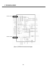
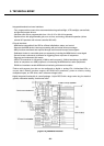
3.4 LO generation and distribution circuits
The integrated LO generation and distribution circuits are driven by internal VCOs to support various
modes to yield highly flexible quadrature LO outputs that drive all GSM and UMTS band upconverters
and downconverters; with the help of these LO generation and distribution circuits, zero-IF architecture
is employed in all GSM and UMTS band receivers and transmitters to translate the signal directly from
RF to baseband and from baseband to RF.
Two fully functional fractional-N synthesizers, including VCOs and loop filters, are integrated within the
RTR6275 IC. The first synthesizer (PLL1) creates the transceiver LOs that support the UMTS
2100/1900/1800 transmitter, and all four GSM band receivers and transmitters including: GSM 850,
GSM 900, GSM 1800, and GSM 1900. The second synthesizer (PLL2) provides the LO for the UMTS
2100/1900/1800 receiver. An external TCXO input signal is required to provide the synthesizer
frequency reference to which the PLL is phase and frequency locked. The RTR6275 IC integrates
most of PLL loop filter components on-chip except two off-chip loop filter series capacitors, and
significantly reduces off-chip component requirement. With the integrated fractional-N PLL
synthesizers, the RTR6275 has the advantages of more flexible loop bandwidth control, fast lock time,
and low-integrated phase error
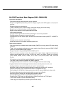
3.5 Off-chip RF Components
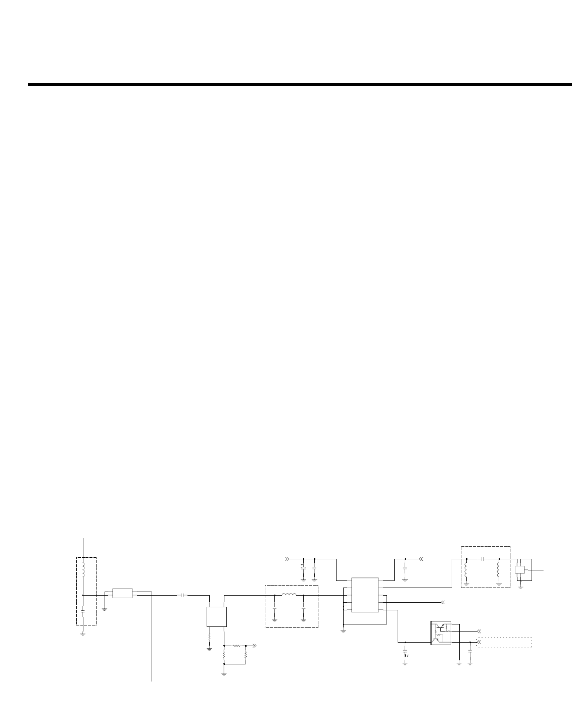
3.5.1 WCDMA PAM (U103: WS2512-TR1G)
The UMTS PA output power is monitored by l power detector circuits(U100 : RTR6275) .
This detector voltage can be used for transmitter calibration and monitor to meet RF system
3. TECHNICAL BRIEF
- 25 -
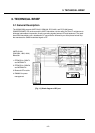
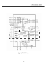
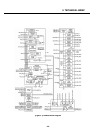
[Figure 1.5] WCDMA PAM, Duplexer, Coupler
20dB
Rev_1.0
Rev.B
Rev_1.0
Rev.D
WCDMA
7dB
0.5p
L125
FL102
EFCH1950TDF1
2
G1
3
G2
5
G3
1
IN
4
O1
U102
CP0402A1950DNTR
50OHM
4
3
COUP
2
IN
1
OUT
L404
1.8nH
45
31
NA
L122
KRX102U
TR100
2
1p
C165
3.3p
C162
C159
15p
R122
130
R11951
1.5p
C154
41
RX
TX
2
FL104
ACMD-7602
ANT
3
PGND
130
R121
0.1u
C170
4.7u
C155
47
R120
2
RFOUT
8
1
VCC1VCC2
10
4
VCONT
5
VREF
WS2512_TR1G U103
11
BGND
GND1
3
GND2
6
7
GND3
9
GND4 RFIN
0.5p
C164
100p
C192
C158
15p
1nH
L123
10nH
C157
+VPWR
PA_R0
+VPWR
PWR_DET
PA_ON
VREG_TCXO_2.85V