


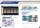
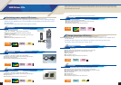
Integrated System in Board is a type of SiP (system in package) technology, and is a module technology that achieves high
densities and thinner form factors by using SANYO's unique substrate and mounting technologies. The Integrated System in
Board lineup consists of three types of process: ISB-Solo, ISB-Duo, and ISB-Quad. Which process is used is selected based on
the application.
In addition to standard products, customer specified circuit blocks can also be converted to Integrated System in Board using an
optimal process, thus creating a new module device in a short time.
76
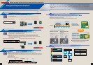
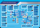
Integrated System in Board
Integrated System in Board
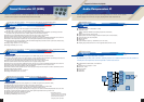
● Thickness of only 0.45 mm (0.65 mm if resistors are included) realizes excellent thermal radiation and
short development TAT
● Optimal for SiP implementation of small-scale block that includes semi-power semiconductors.
● Adopts unique SANYO-developed 0.2 mm thickness high-density substrate (2 layers)
Line 40
µm / Space 40 µm at 25 µm thickness copper foil,
Via diameter 100 µm / Via land diameter 150 µm
● Thickness of only 0.53 mm (0.73 mm if resistors are included) realizes high-density mounting
● Optimal for SiP implementation of high-frequency (up to 10 GHz) blocks, blocks that require
performance or EMC workarounds based on component placement/wiring pattern, and blocks that
require partial high-density mounting.
●Adopts unique SANYO-developed 0.24 mm thickness high-density substrate (4 layers)
●Thickness of only 0.6 mm realizes high-density mounting
●Optimal for SiP implementation of high-frequency (up to 10 GHz) blocks, blocks that require performance
or EMC workarounds based on component placement /wiring pattern, and subsystems that require high-
density mounting.
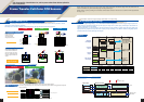
●Chip-on-Board type
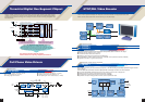
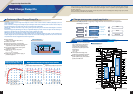
■ Assembly structure examples
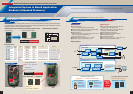
Integrated System in Board
Earlier mounting
Integrated System in Board
Top surface
Back surface
Mounting area
reduced by 80%
4.45 × 4.45 × 0.65 mm
3
Integrated System in Board
Earlier mounting
Integrated System in Board
Top surface
Back surface
Mounting area
reduced by 58%
4.3 × 4.3 × 0.73 mm
3
Passive components
(resistors and capacitors)
ISB-Duo
ISB-Quad
WS-CSP Flip Chip
0.24 mm
■ Application example (Cell phone charger circuit block)
■ Application example (Clock detector block)
■ Assembly structure examples
■ Assembly structure examples
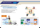
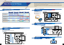
● Reduced wiring area due to implementation as miniature modules
● Integration of noise reducing components
● Supply voltage stabilization by using dedicated layers for power supply and ground
Dedicated power
supply/ground layer
Integration of noise
reducing components
LSI
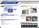
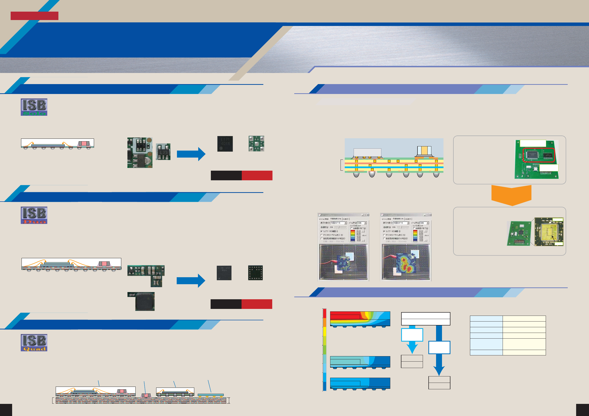
Analysis conditions
Chip heat generation
Chip size
Land size
Atmospheric temperature
Cooling conditions
Analysis model
3 [W]
4✕4✕0.3 [mm
3
]
5✕5✕0.03 [mm
3
]
25 [°C]
Ideal cooling of the solder lower
surface;
25 [°C]
1/4 model (since symmetrical)
Maximum
temperature
40.4 [°C]
Maximum
temperature
54.3 [°C]
Maximum temperature
92.7 [°C]
Temperature
difference
38.4°C
Temperature
difference
52.3°C
MK
Z
Y X
MK
Z
X
Y
MK
X
Y
97
81
65
49
33
89
73
57
41
25
Typical BGA
Integrated System Board
that dissipates heat
Integrated System Board package
Integrated System in Board Process Lineup
ISB-Solo
ISB-Duo
ISB-Quad
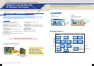
Noise suppression effect (measured)
Heat dissipation effect (simulation)
Module technologies that achieve high-density and thinner form factors
SANYO Original technology
■ Evaluation results using a microcontroller and SRAM
(Surface probe method - 30 MHz to 1 GHz)
SRAM
10 mm × 10 mm
SRAM
Noise is reduced
significantly
Microcontroller
Microcontroller
Wiring on board
Integration of noise
reducing components
Integrated System in
Board stack structure
(high-density mounting)
Integration of noise
reducing components
Reasons noise can be reduced by Integrated Sysytem in Board
ISB-Duo (2-layer ISB)
Separate microcontroller
and SRAM
Surface scan using a field probe