


SANYO fabricates frame transfer (FT) CCD sensors using unique technologies with ultrafine design rules and provides them as
modules assembled using advanced leading-edge mounting technologies.
SANYO makes a point of providing fine and delicate semiconductor devices in forms that our customers will find approachable
and easy to use.
1312
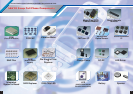
High image quality, ultraminiature size, and low power makes these devices optimal for
use in cell phones
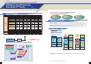
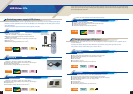
Frame Transfer Full-Color CCD Sensors
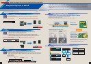
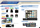
Achieves the industry’s smallest optical size class by using the frame transfer CCD, which makes it possible to reduce
feature sizes while maintaining sensitivity.
Sensitivity was increased by adopting a simple single-layer gate gap structure and thin-film polysilicon.
Photo Diode
Micro Lens
Photo Diode
Micro Lens
P-Sub
N+ N+P+ P+ N+ N+
Micro Lens
Photo Diode
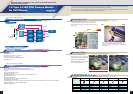
[storage 1/3 compression Type]
Imaging area
Storage area
Horizontal shift register
output
PD
=Transfer
area
Low voltage
Imaging area
Horizontal shift register
output
High voltage
Transfer
area
Switch
PD
Low voltage
X direction register
Y direction register
PD
Amplifier
PD: Photo Diode
FT-CCD CMOS IL-CCD
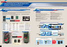
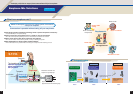
A charge pump type voltage step-up circuit that features minimal noise generation, and the supply voltages required for
system drive are generated efficiently with just the supply of a single +2.9 V power supply. This design is also effective at
achieving reduced power consumption.
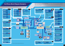
SANYO implemented, in a single package, the timing generator circuit required for system drive and all the analog and
digital processing required to accept the CCD output by taking advantage of the SANYO CMOS analog/digital hybrid
process and MCP (multi-chip package) technologies.
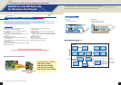
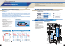
CCD sensor CMOS sensor (1/4 VGA)
2004 2005 2006
Megapixel
CCD chipset
1.0M
VGA CCD
chipset
Coexistance
between
near infrared
sensitivity and
color
3.2M
CIF CCD
chipset
Near infrared
CCD chipset
30 fps
High reliability
LC99807
LC99808
LC99117
LC99268
LC99267
LC99810
LC99353
LC99812
LC99359
LC99704
LC99268G
LC99809
LC99268FL
Near infrared
High image quality
Dynamic range of
VGA motion picture
and 3.2-MP still picture
has expanded
Inproved stability
at high-temperature
(85 °C)
Still Motion Still Motion Motion
Motion
Motion
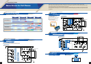
LC99359 3.2M VGA Low High Normal 30 DigitalColor
LC99268FL VGA VGA High
Wide 15 DigitalColor
LC99117 CIF CIF
Very High
Wide 30 DigitalB&W
Dynamic Range
Frame Rate
Output
Resolution
Sensitivity
Color/B&W
Chip Set
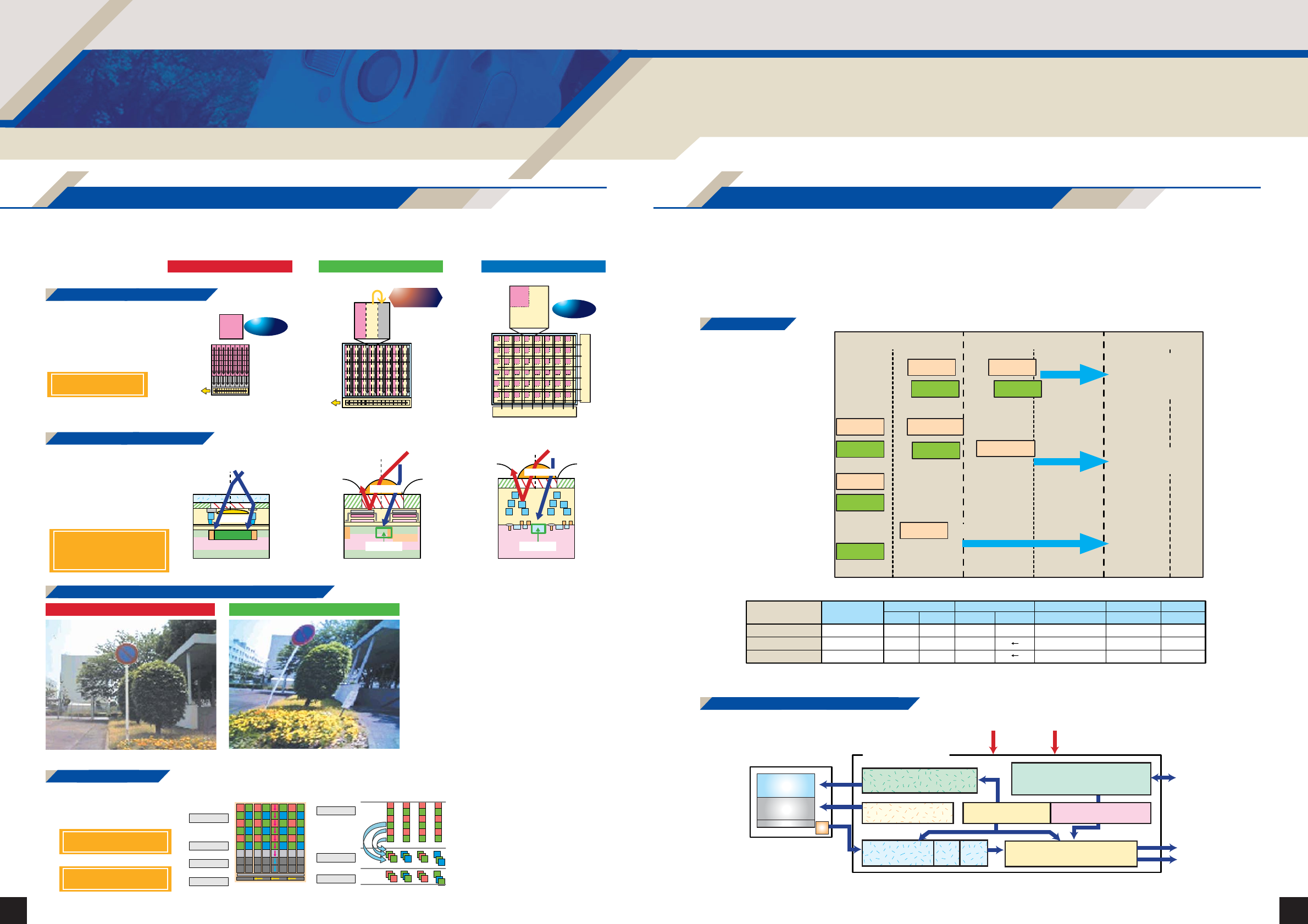
Correlated double
sampling
CCD driver
Charge pump
Power supply circuit
Digital color signal processor
RGB/YUV output
Multifunction DSP
CCD module
CCD timing generator
+2.9 V
Single power supply
Storage area
Imaging area
Horizontal shift
register
Output
amplifier
AGC
8-bit
ADC
Analog front end processor
Registers for picture arrangement
/Output mode/etc.
I
2
C bus
AE/AWB controller
CLK
HREF/VREF
High sensitivity
Horizontal transfer
FT-CCD structure
Mixing area
2R+G B+2G
R, G, and B are extracted by calculations
Compressed to 1/3 the number of lines by combining 3 pixels.
R+2G 2B+G
Low moire
Imaging area
Imaging area
Storage area
Storage area
Mixing area
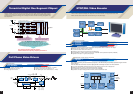
Frame Transfer CCD
CCD drive circuit and image processing implemented in a single package
Multifunction DSP chip
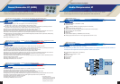
Device Density Comparison
Roadmap
Cross Section Comparison
Newly developed
Comparison of Differences in Electronic Shutter Types
CCD Module Basic Structure Example
Comparison of chip
sizes required to
acquire the same
imaging device area
The FT CCD method uses
no elements that block the
entrance of light, and thus
they can capture light from
a wider range of incidence
angles.
High sensitivity
Reducing the device
height is possible
In the 1.0-MP CCD, SANYO developed a new charge accumulation method.
Low moire, high sensitivity, and a high frame rate achieved by pixel addition during preview and spatial
filter processing.