


18
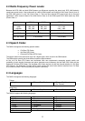
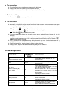
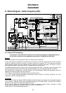
FLEX-BO ARD
RF
BLOCK
1
DGND
2
CHG
3
GEN I/O
4
POWER OUT
5
RX (IN)
6
TX (OUT)
7
ACC ID
8
RTS
9
CTS
10
AUDIO OUT
11
AUDIO IN
12
AGND
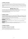
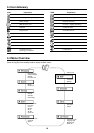
SIM I/F
HFK I/F
SIM LEVEL
CTRL 3V/5V
A/D CONV RF I/F A/D, D/A
SIM
Connector
Battery
Connector
KEY-LED
LCD-LED
KEY-MATRIX
SLIDE-SW
(REC/LOCK
or Manner
)
*Ringer
*Vibrator
*Loud-
Speaker
MIC
32kHz
CLK-
CTRL
RTC / ID
SIM CARD
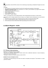
IC 1
FLASH/SRAM
LCD
SIM
Interface
MCP-I/F
KEY-I/F
HEADPHONE-JACK
JOG-I/F
RF-I/F
MODEM-I/F
LCD-I/F
TIME
PROCCESSING
UNIT
RTC
IC 2
I/F
AUDIO
AMP
I/O CONNECTOR
AUDIO
I/F
MIC
KEYBOARD
JOG DIAL
AUDIO
AMP
HEADSET
AUDIO &
REMOTE
RINGER
JOG
Power / CHG
Management
IC 1
I/F
EAR
RECEIVER
LI-ION
BATTERY
TCXO
IC 2
Multiactor
BL-I/F
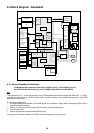
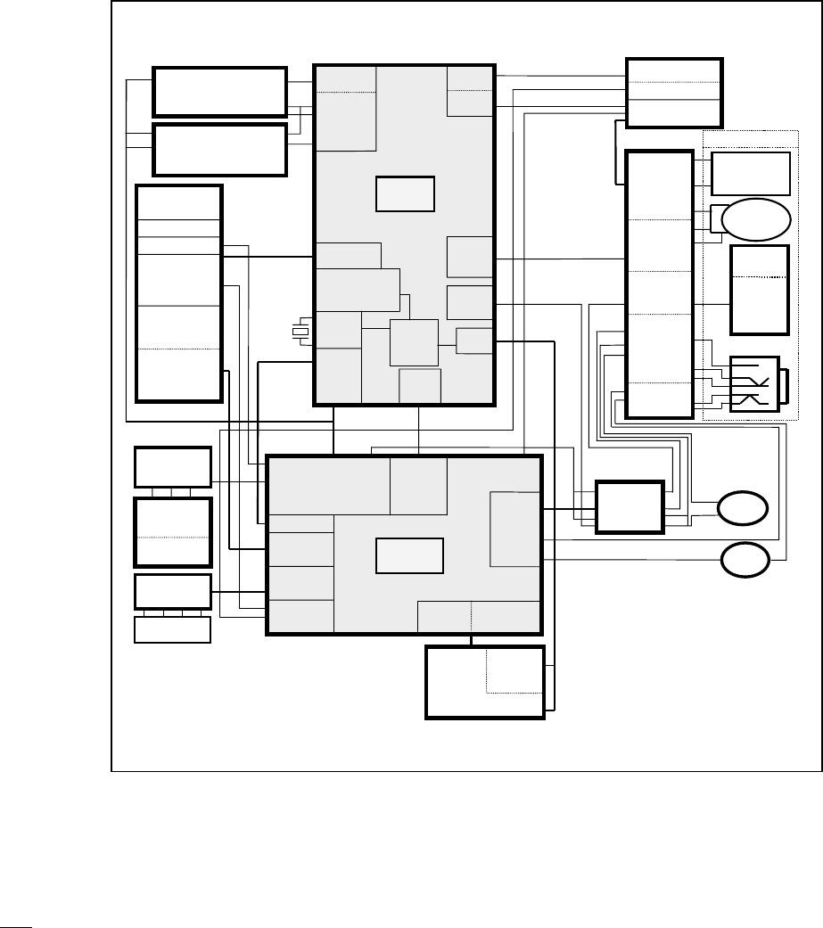
6.2 Block Diagram - Baseband
6.2.1 General Baseband Indications
The Baseband part consists of two chips, a digital chip IC 1 and an analog one IC 2.
The CMD-J5/J16 external memory size is 32 Mbits Flash ROM and 4 Mbit SRAM.
IC 1
The application of IC 1 is the management of the GSM baseband processes through the GSM layer 1, 2 and 3
protocols as described in the ETSI standard with a specific attention to the power consumption in both GSM
dedicated and idle modes.
It is a chip that implements:
the digital baseband processes of the CMD-J5/J16 and combines a Digital Signal Processing (DSP) with its
program and data memories,
a Micro-Controller core with emulation facilities and an internal RAM memory,
a clock squarer cell,
several compiled ports and equivalent CMOS gates.
Full support for Full-Rate, Enhanced Full-Rate and Half-Rate speech coding is given.