SAMSUNG Proprietary-Contents may change without notice
Circuit Description
5-2
This Document can not be used without Samsung's authorization
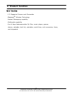
- TX Function
The device implements Skyworks Polar Loop transmit architecture. This architecture
autonomously splits the amplitude and phase within the device using the traditional
analog In-Phase and Quadrature (I/Q) signals. The filter-saving advantage of the
translation-loop approach is embedded in the architecture. Also included is an AM loop
that provides both signal AM and power level control. The transmitter is provided a
coupled feedback signal from the PA and downconverts it to an IF. Following an IF VGA,
this feedback signal is fed to both loops. The reference for both loops is a transmit IF
signal produced by an I/Q modulator
5. POWER AMP (PAM400)
The module consists of a EGSM850/900 PA block and a DCS1800/PCS1900 PA block,
Both PA blocks share common power supply pins to distribute current. The subsystem
consists of two parts : a Power Amplifier Control (PAC) block, and an Integrated Coupler.
To select GSM900/850 and GMS1800/1900 as determined from the Band Select
(BAND_SEL) signal. SKY77331 contains band select switching circuitry to select GSM
(BAND_SEL is low) and DCS/PCS (BAND_SEL is HIGH) as determined from the Band
Select (BAND_SEL) signal. The BAND_SEL pad selects the PA output (DPCS_OUT or
GSM_OUT) while the Power Control (VPC) controls the level of output power. The
integrated power amplifier control (PAC) function provides envelope amplitude control by
reducing sensitivity to input drive, temperature, power supply, and process variation.
< Baseband Circuit description of SGH-D407 >
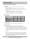
1. CSP2750 (UCD301)
==> The CSP2750 has two major logical components power management and
conversion signal processing.
The PSC component is responsible for all power-related functionality, including the
following;
●
Power management for RF, BB and ancillary devices within the GSM/GPRS
●
Battery-charge management
●
Reset control
●
SIM card voltage-level shifting
The CSP component is responsible for the following ;
●
Intraframe event scheduling
●
Voice band processing, including voice band ADC and DAC
●
Analog baseband processing, including baseband ADC and DAC
●
Providing RF interface for Trident digital baseband device
●
Transmitter Power control
●
Automatic frequency control
●
A5 ciphering
●
Low-power sleep mode and wake-up control
The CSP2750 has the following major physical components;


