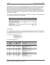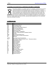
GTR64 http://www.matrix.es/GTR64
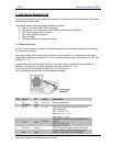
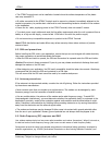
10
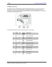
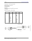
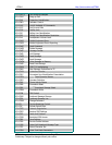
RI1
IO 8
O
I/O
0.4 – 3.2 V
-0.5 - VREF
Ring Indication
Digital Input/Output I/O 8
11 IO 2 I/O -0.5 - VREF
Digital VREF
Digital Input/Output I/O 3
12 IO 4 I/O -0.5 - VREF
Digital Input/Output I/O 4
Digital VREF
13 CE
signal
SERVI I -0.5 - +3.6V
Flash programming enable
Active High
14 GND 0V Ground connection
15
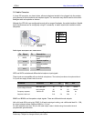
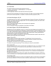
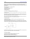
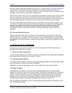
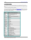
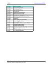
3.7.1. SECONDARY SERIAL PORT
secondary serial por UART3.
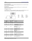
ADC 1 I 0 - 2.59V ADC Input 1
The
t is called
Pin Name Direction Function
2 RD3 I ±5 v
RS232 UART signal:
Secondary
Transmitted data
3 TD3 o ± 25V
Secondary RS232 UART signal
Received data.
V IL < 0.6V, V IH > 2.4V
T sists a fu al com transmission and reception lines.
in electrical sig acteristic r UART1, including the baud rate range
th ilit au
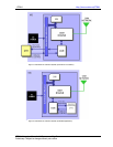
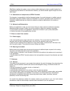
.7.2. I2C Serial Control Bus
ace signals, SDA (data) & SCL (clock), they utilize a different type
f level-shifting technology to that of the ‘common’ IO. The I2C level shifter IC uses an open drain
ited to bi-directional low voltage I2C port translation to the
ormal 3.3 V or 5.0 V I2C-bus signal levels. Unlike the common level shifters, the I2C level shifters have
y 5oh resistance betwee d output pins.
The I2C level shifters use VREF as the host-si nal 1.8V digital IO core
the module-side reference.
ace comprises tw als; data and SCL have pull-up
ist erefore, when the e, bot e.
ue to the wired-AND function, the SCL line will be held LOW by the
d. Therefore, the device with the shorter LOW period will be in a HIGH
UAR
Tim
3 con
g and
of ll duplex seri
nals char
munication port with
s are the same as fo
and
e capab y to to-baud.
3
Because of the nature of the I2C interf
o
construction with no direction pin, ideally su
n
a ver low (6. m RDSON) n input an
de voltage reference and the inter
as
The I2C interf
res
o sign
bus is fre
(SDA) and clock (SCL). Both SDA
ors. Th h SDA and SCL are in a HIGH stat
T
he GTR64 implementation of I2C supports only a single master mode, with the module being the
master. The output stages of SDA and SCL must have an opendrain or open-collector to perform a
wired-AND function. The wired-AND function provides the I2C bus ability to perform clock
synchronization on the SCL line. D
device with the longest LOW perio
wait-state during this time.
GTR64 Integrators Manual V.1.2 Pag. 20
Preliminary. Subject to change without prior notice