GTR64 http://www.matrix.es/GTR64
Clock synchronization can be used as a handshaking mechanism, to enable receivers to cope with fast
data transfers. On a byte level, a slave (host application-side) I2C device may be able receive a data
transfer, but need time to store the byte received before it is ready to receive another byte. The
slave/receiver will therefore hold the SCL line low, after sending the acknowledge bit following the byte
received, thereby forcing the master into a wait state. Once the SCL is re
leased by the slave/receiver,
e wait state of the master will end. This feature of the I2C standard is known as clock-stretching and
he I2C interface supports Standard-mode (100kbps) and Fast-mode (400kbps). It also supports Normal
.
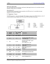
SPI uses the same command structure as the AT command AT*E2SPI. The
mentation of this function only supports SPI Mode 0 (data is latched on a rising clock edge
e used - CLOCK (IO1 pin),
DATA INPUT (IO2 pin),
DATA OUTPUT (IO3 pin),
3.7.4
th
is supported by the GTR64.
T
(7-bit) addressing and Extended (10-bit) addressing
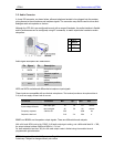
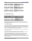
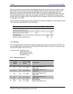
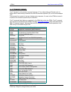
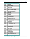
Parameter Min Typ Max Unit
SCL clock frequency 0 400 kHz
LOW period of the SCL clock 1.3 μs
HIGH period of the SCL clock 0.6 μs
3.7.3. SPI Bus
SPI: The implementation of
current imple
and the default state of the clock is low).
4 wires ar
and SYNC (RI pin).
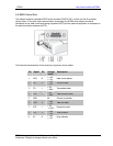
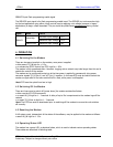
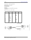
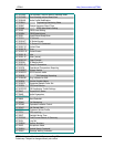
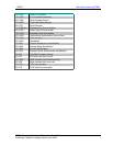
. General Purpose IO
Pin
GTR64
Signal
Dir
Max. Voltage
limits
Description
4 IO 1 I/O -0.5 - VREF
Digital Input/Output I/O 1
Digital VREF
11 IO 2 I/O -0.5 - VREF
Digital Input/Output I/O 2
Digital VREF
5 IO 3 I/O -0.5 - VREF
Digital Input/Output I/O 3
Digital VREF
12 IO 4 I/O -0.5 - VREF
Digital Input/Output I/O 4
Digital VREF
1
I/O -0.5 - VREF Dig
0
RI1
IO 8 ital Input/Output I/O 8
O 0.4 – 3.2 V Ring Indication
Data hold time 0 0.9 μs
Capacitive load for each bus line 400 pF
GTR64 Integrators Manual V.1.2 Pag. 21
Preliminary. Subject to change without prior notice