


MB3891
24
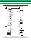
(8) LDO5
The LDO5 circuits uses the reference voltage supply and generates an output voltage (2.8 V typ.) at the OUT5
terminal (pin 57) when the OUT1 terminal (pin 12,13) is in output state and an “H” level signal is input at the
CONT5 terminal (pin 57). Power can be drawn from the OUT5 terminal for external use, up to a maximum load
current of 50 mA.
(9) LDO6
The LDO6 circuit uses the reference voltage supply and generates an output voltage (2.1 V typ.) at the V-BACKUP
terminal (pin 21). Power can be drawn for external use, from the V-BACKUP terminal, up to a maximum load
current of 250 µA.
(10) REF-OUT
This circuit uses the reference voltage generated by the reference voltage block (1.225 V typ.) to produce a
temperature compensated reference voltage (1.225 V typ.) at the REF-OUT terminal(pin 24) by means of a
voltage follower. The reference voltage can also be drawn from the REF-OUT terminal for external use, up to a
load current of 50 µA.
(11) VSIMOUT Chargepump
The VSIMOUT charge pump uses the voltage from the battery and generates 5.0 V (typ.) voltage at the VSIMOUT
terminal (pin 29) when an “H” level signal is input at the SIMPROG terminal (pin 27) , or 3.0 V (typ.) voltage
when an “L” level signal input at the SIMPROG terminal. This voltage can also be drawn from the VSIMOUT
terminal for external use, up to a load current of 10 mA.
(12) GSM/SIM Logic Translation
µ
P Interface
When a signal is input from the microprocessor to the RESET-IN terminal(pin 33) and CLK-IN terminal (pin 34),
a level-shifted voltage is output from the RST terminal (pin 36) and CLK terminal (pin 37) to the SIM card. The
µP-IO terminal (pin 35) and SIM-IO terminal (pin 38) are input/output pins and carry signals between the
microprocessor and SIM card.
(13) SIM Interface 5 V (SIMPROG
=
“H”)
When an “H” level signal is input to the SIMPROG terminal (pin 27), 5.0 V (typ.) voltage is generated from the
VSIMOUT terminal (pin 29) as a power supply for the SIM card.
(14) SIM Interface 3 V (SIMPROG
=
“L”)
When an “L” level signal is input to the SIMPROG terminal (pin 27), 3.0 V (typ.) voltage is generated from the
VSIMOUT terminal (pin 29) as a power supply for the SIM card.
■
■■
■
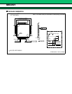
SETTING THE XPOWERGOOD TIME
When the OUT1 terminal (pin 12,13) voltage exceeds 2.0 V (typ.), the capacitor (CDELAYCAP) connected to the
DELAYCAP terminal (pin 18) starts charging, the XPOWERGOOD terminal (pin 17) voltage rises. The XPOW-
ERGOOD terminal voltage rising time (XPOWERGOOD time) can be set by a capacitor connected to the
DELAYCAP terminal.
XPOWERGOOD time : T
XPG (s) := 0.8 × CDELAYCAP (µF)