


MB3891
3
■
■■
■
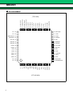
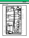
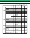
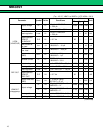
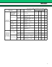
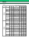
PIN DESCRIPTION
(Continued)
Pin No. Symbol I/O Descriptions
1, 2 N.C. Non connection.
3, 4 OUT3 O LDO3 output pin.
5GND3 LDO3 ground pin.
6, 7 OUT2 O LDO2 output pin.
8, 9, 10, 11 VBAT1 Battery voltage input pin for LDO1 and LDO2.
12, 13 OUT1 O LDO1 output pin.
14 CONT1 I Power on input from keypad (Active low, Pulled up to VBAT2).
15 CONT6 I “CONT6” input from digital system µP (Active high).
16 CONT2 I External accessory supply voltage Enable (Active high).
17 XPOWERGOOD O Generates the main reset. (Active low, when OUT1 is out of regulation).
18 DELAYCAP Timing capacitor for XPOWERGOOD delay.
19 GND1 LDO1, LDO2, V-BACKUP, Reference and System ground pin.
20 VBAT2
Battery voltage input pin for both UVLO’s, Reference and V-BACKUP
LDO.
21 V-BACKUP O Supply voltage for Charger for rechargeable Lithium coin cell.
22 VREF O Supply voltage for Reference.
23 VFIL O Reference voltage Filter.
24 REF-OUT O Reference output voltage (Present when BACKUP UVLO is high).
25 VCC-VSIM Input voltage for charge pump. (Supplied by VBAT1).
26 VSIM-ON I VSIM supply Enable (Active high).
27 SIMPROG I VSIM programming: Low = 3 V SIM, High = 5 V SIM.
28 OSC Oscillator output pin.
29 VSIMOUT O Supply voltage for 3 or 5 V SIM-Card (SmartCard).
30 VCAP+Positive side of boost capacitor.
31 VCAP−Negative side of boost capacitor.
32 GND-VSIM 3 or 5 V SIM-Card (SmartCard) ground pin.
33 RESET-IN I Non level shifted SIM reset (µP side).
34 CLK-IN I Non level shifted clock (µP side).
35 µP-IO I/O Non level shifted bi-directional data input/output (µP side).
36 RST O Level shifted SIM reset (SmartCard side).
37 CLK O Level shifted SIM clock (SmartCard side).
38 SIM-IO I/O Level shifted bi-directional SIM data input/output (SmartCard side).
39 GND4 LDO4 ground pin.
40, 41 OUT4 O LDO4 output pin.