


MB3891
6
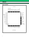
■
■■
■
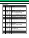
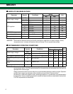
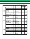
ABSOLUTE MAXIMUM RATINGS
* : The packages are mounted on the dual-sided epoxy board(10 cm × 10 cm)
WARNING: Semiconductor devices can be permanently damaged by application of stress (voltage, current,
temperature, etc.) in excess of absolute maximum ratings. Do not exceed these ratings.
■
■■
■
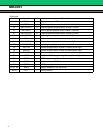
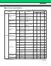
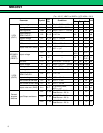
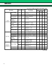
RECOMMENDED OPERATING CONDITIONS
WARNING: The recommended operating conditions are required in order to ensure the normal operation of the
semiconductor device. All of the device’s electrical characteristics are warranted when the device is
operated within these ranges.
Always use semiconductor devices within their recommended operating condition ranges. Operation
outside these ranges may adversely affect reliability and could result in device failure.
No warranty is made with respect to uses, operating conditions, or combinations not represented on
the data sheet. Users considering application outside the listed conditions are advised to contact their
FUJITSU representatives beforehand.
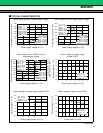
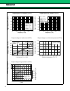
Parameter Symbol Conditions
Rating
Unit
Min. Max.
Power supply voltage
VBAT −0.3 7 V
VCC-VSIM −0.3 7 V
LDO regulator
I
O OUT1 pin 120 mA
IO OUT2 pin 50 mA
I
O OUT3 pin 100 mA
I
O OUT4 pin 100 mA
IO OUT5 pin 50 mA
VSIMOUT chargepump I
O VSIMOUT pin 10 mA
Power dissipation P
D Ta ≤ +25 °C 800* mW
Storage temperature Tstg −55 +125 °C
Parameter Symbol Conditions
Value
Unit
Min. Typ. Max.
Power supply voltage
VBAT 3.0 3.6 5.5 V
VCC-VSIM 3.0 3.6 5.5 V
LDO capacitor guarantee value C
O OUT1 to OUT5, V-BACKUP pin 0.8 1.0 µF
REF-OUT capacitor guarantee
value
CO REF-OUT pin 0.027 µF
VSIMOUT capacitor guarantee
value
C
O VSIMOUT pin 10 µF
Operating ambient temperature Ta −20 +25 +85 °C