


NWZ-A826/A826K/A828/A828K/A829
NWZ-A826/A826K/A828/A828K/A829
1919
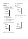
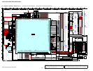
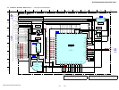
For Schematic Diagrams.
Note:
• All capacitors are in μF unless otherwise noted. (p: pF)
50 WV or less are not indicated except for electrolytics
and tantalums.
• All resistors are in Ω and
1
/4 W or less unless otherwise
specifi ed.
• C : panel designation.
THIS NOTE IS COMMON FOR PRINTED WIRING BOARDS AND SCHEMATIC DIAGRAMS.
(In addition to this, the necessary note is printed in each block.)
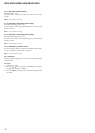
• A : B+ Line.
• Power voltages is dc 3.7 V and fed with regutated dc pow-
er supply fron CN901 pin 1 and 2 on the MAIN board.
• Voltages and waveforms are dc with respect to ground
under no-signal conditions.
no mark
: PLAY BACK
• Waveforms is taken with a oscilloscope.
Voltage variations may be noted due to normal production
tolerances.
• Voltages are taken with VOM (Input impedance 10 MΩ).
• Voltage variations may be noted due to normal production
tolerances.
• Circled numbers refer to waveforms.
• Signal path.
F : AUDIO
L : VIDEO
• The voltage and waveform of CSP (chip size package)
cannot be measured, decause its lead layout is different
form that of conventional IC.
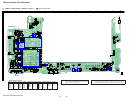
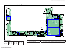
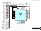
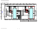
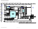
For Printed Wiring Boards.
Note:
• X : Parts extracted from the component side.
• : Pattern from the side which enables seeing.
(The other layers' patterns are not indicated.)
Caution:
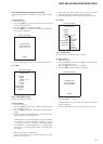
Parts face side:
(SIDE A)
Pattern face side:
(SIDE B)
Parts on the parts face side seen from
the pattern face are indicated.
Parts on the pattern face side seen from
the parts face are indicated.
• MAIN and SW boards are mulyi-layer printed board.
However, the patterns of intermediate-layers have not been
included in diagrams.
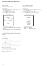
• Indication of transistor.
C
B
These are omitted.
E
Q
• Lead layouts
surface
CSP (Chip Size Package) Lead layout of conventional IC