


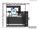

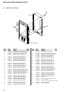

NWZ-A826/A826K/A828/A828K/A829
39
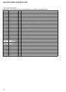
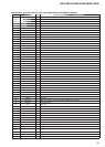
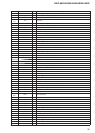
Pin No. Pin Name I/O Description
U1 to U5 SDR_A12 to SDR_A8 O Address signal output to the SD-RAM
U8 SDR_CASZ O Column address strobe signal output to the SD-RAM
U9 GND - Ground terminal
U10 to
U12
NC - Not used
U13 WAKEUP O Wake up signal output terminal
U14 PSM_LODET O USB power control signal output terminal
U15 L1_DET - Not used
U16 ERR_RST_REQZ - Not used
U17 NC - Not used
U18 REFCLKO O Master clock signal output to the A/D, D/A converter
U19 NC_OUT_SEL O Line output selection signal output terminal Not used
U22 C_TDO O Data output terminal for JTAG
U23 VLOGIN I Power supply input terminal (+2.9 - 4.2V)
U24 C_TCK I Clock signal input terminal for JTAG
U25 VPLL O Power supply output terminal (+1.2V)
U26 CKI I Main system clock input terminal (11.2896 MHz)
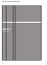
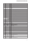
V1 to V3 IO_A - Not used
V4, V5 SDR_A6, SDR_A5 O Address signal output to the SD-RAM
V8 SDR_A7 O Address signal output to the SD-RAM
V9 GND - Ground terminal
V10 CHG_XCHGEN O Charge enable signal output to the power control
V11 NC - Not used
V12 to V15 GND - Ground terminal
V16 DSP_DET - Not used
V17 LCD_BLTCTL O LCD back light control signal output to the LED control
V18 UART_SEL O Serial data select signal output to the multiplexer
V19 NCHP_DET I Headphone detection signal input terminal Not used
V22 C_RTCK I Clock signal input terminal for JTAG
V23 C_TRSTZ I Reset signal input terminal for JTAG
V24 VPLLIN I Power supply input terminal (+2V)
V25 VDSPIN I Power supply input terminal (+2.9 - 4.2V)
V26 VDSP - Not used
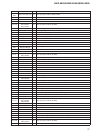
W1 IOGND - Ground terminal
W2 NC - Not used
W3 LCD_PON O Reset signal output to the liquid crystal display
W4, W5 SDR_A4, SDR_A3 O Address signal output to the SD-RAM
W8 CHG_PEN2 O Charge enable signal output to the power control
W9 GND - Ground terminal
W10 NC - Not used
W11 to
W18
GND - Ground terminal
W19 WR_ERR - Not used
W22 NC_PLUG_PWR O Power control signal output terminal Not used
W23 C_TDI I Data input terminal for JTAG
W24, W25 IO_B - Not used
W26 VLO O Power supply output terminal (+1.2V)
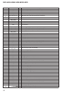
Y1 IOVDD I Power supply input terminal (+2.85V)
Y2 CHG_ICTL O Charge control signal output to the power control
Y3 HP_XMUTE O Analog muting control signal output terminal
Y4, Y5 SDR_A2, SDR_A1 O Address signal output to the SD-RAM
Y22, Y23 TM1, TM0 - Not used
Y24, Y25 VDD_DSP I Power supply input terminal (+1.2V)
Y26 VHP O Power supply output terminal (+2.9V)
AA1 CRD_LINEOUT O Line output selection signal output terminal
AA2 WAKEUP_INT I Wake up signal input terminal