


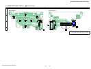
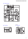


NWZ-A826/A826K/A828/A828K/A829
37
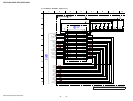
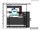
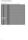
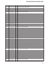
Pin No. Pin Name I/O Description
G23 to
G25
AB0_D15 to AB0_D13 I/O Two-way data bus with the USB controller
G26 NC - Not used
H1 USBSUSPD - Not used
H2 NC - Not used
H3 to H5
SDR_DATA25,
SDR_DATA27,
SDR_DATA31
I/O Two-way data bus with the SD-RAM
H8 NAND_RBZ1 O Read/busy signal output to the NAND fl ash memory (NWZ-A828/A828K/A829 only)
H9 BT_XRST O Reset signal output to the bluetooth controller
H10 BT_PWRCTL O Power control signal output terminal for the bluetooth section
H11, H12 NC - Not used
H13 NC_PWRON O Power control signal output terminal Not used
H14, H15 NC - Not used
H16 AB0_WRZ O Write strobe signal output to the USB controller
H17 NC - Not used
H18, H19 AB0_A1, AB0_A2 O Address signal output to the USB controller
H22 to
H25
AB0_D8, AB0_D9,
AB0_D7, AB0_D6
I/O Two-way data bus with the USB controller
H26 NC - Not used
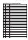
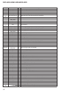
J1 to J3 IO_A - Not used
J4, J5
SDR_DATA29,
SDR_DATA30
I/O Two-way data bus with the SD-RAM
J8 NAND_RBZ2 O Read/busy signal output to the NAND fl ash memory (NWZ-A829 only)
J9 BT_LEDCTL2 O LED drive signal output terminal for the bluetooth indicator
J10 SPI_CS_SEL O Chip select signal selection signal output terminal Not used
J11 to J17 GND - Ground terminal
J18 NC - Not used
J19 AB0_RDZ O Read strobe signal output to the USB controller
J22 to J24 AB0_D10 to AB0_D12 I/O Two-way data bus with the USB controller
J25 CHGGND1 - Ground terminal
J26 NC - Not used
K1 to K3 VDD_L1 I Power supply input terminal (+1.2V)
K4, K5
SDR_DATA28,
SDR_DATA26
I/O Two-way data bus with the SD-RAM
K8 NAND_RBZ3 O Read/busy signal output to the NAND fl ash memory (NWZ-A828/A828K/A829 only)
K9 NAND_DA6 I/O Two-way data bus with the NAND fl ash memory
K10 to K18 GND - Ground terminal
K19 NC - Not used
K22 LCD_HSYNC O Horizontal sync signal output to the liquid crystal display
K23 LCD_ENABLE O Enable signal output to the liquid crystal display
K24 LCD_VSYNC O Vertical sync signal output to the liquid crystal display
K25 CHGGND2 - Ground terminal
K26 NC - Not used
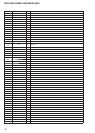
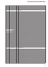
L1 to L5
SDR_DATA23 to
SDR_DATA20,
SDR_DATA24
I/O Two-way data bus with the SD-RAM
L8 SDR_DATA19 I/O Two-way data bus with the SD-RAM
L9 NAND_DA4 I/O Two-way data bus with the NAND fl ash memory
L10 GND - Ground terminal
L11 NC - Not used
L17, L18 GND - Ground terminal
L19 LCD_B1 O RGB video (blue) signal output to the liquid crystal display
L22 to L25 LCD_B2 to LCD_B5 O RGB video (blue) signal output to the liquid crystal display
L26 NC - Not used
M1 to M5
SDR_DATA18 to
SDR_DATA14
I/O Two-way data bus with the SD-RAM
M8 SDR_DATA13 I/O Two-way data bus with the SD-RAM