


NWZ-A826/A826K/A828/A828K/A829
40
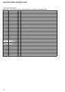
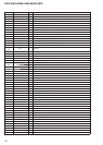
Pin No. Pin Name I/O Description
AA3 TU_STO I Status signal input terminal Not used
AA4 SDR_A0 O Address signal output to the SD-RAM
AA5 SDR_CLK O Clock signal output to the SD-RAM
AA22,
AA23
GND - Ground terminal
AA24 TM2 - Not used
AA25 VANAIN I Power supply input terminal (+2.9 - 4.2V)
AA26 VANA O Power supply output terminal (+2.85V)
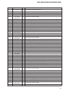
AB1 VDD_L0 I Power supply input terminal (+1.2V)
AB2 TXD_PUCTL I Serial data input terminal
AB3 CRD_DET I Wake up signal input from the WM-PORT connector
AB4 CHG_XFLT I Fault signal input from the power control
AB5 SDR_BA0 O Bank address signal output to the SD-RAM
AB6, AB7 NC - Not used
AB8 USB_SUSPEND O USB suspend signal output to the power control
AB9 IO_C - Not used
AB10 to
AB12
NC - Not used
AB13 USB_XRST O Reset signal output to the USB controller
AB14 USB_INT2 I Interrupt request signal input from the USB controller
AB15 to
AB17
MS_DATA3, MS_
DATA2, MS_DATA0
- Not used
AB18 MS_INSZ - Not used
AB19 WR_LEDCTL - Not used
AB20 PM1_SEN - Not used
AB21 PM1_CLK - Not used
AB22 PM0_SEN I L/R sampling clock signal input from the A/D, D/A converter
AB23,
AB24
GND - Ground terminal
AB25 GND1 - Ground terminal
AB26 OSCIN I Sub system clock input terminal (32.768 kHz)
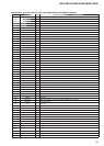
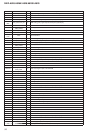
AC1 to
AC3
IO_A - Not used
AC4 XCHG_DET I Charge detection signal input from the power control
AC5 USB_INT1 I Interrupt request signal input from the USB controller
AC6 SPIO_XCS0 O Chip select signal output to the liquid crystal display
AC7 SPI0_SK O Serial data transfer clock signal output to the A/D, D/A converter and liquid crystal display
AC8 SPI0_SO O Serial data output to the A/D, D/A converter and liquid crystal display
AC9 IO_C - Not used
AC10 to
AC13
NC - Not used
AC14 AVDD_LPLL I Power supply input terminal (+1.2V)
AC15 AVDD_HPLL I Power supply input terminal (+1.2V)
AC16 MS_DATA1 - Not used
AC17 MS_BS - Not used
AC18 MS_SCK0 - Not used
AC19 NC - Not used
AC20 ADA_XRST O Reset signal output to the A/D, D/A converter
AC21 PM0_CLK I Bit clock signal input from the A/D, D/A converter
AC22 PM0_SO O Serial audio data output to the A/D, D/A converter
AC23 BT_LEDCTL1 O LED drive signal output terminal for the bluetooth indicator
AC24 VLOIN I Power supply input terminal (+1.8V)
AC25 IO_C - Not used
AC26 OSCOUT O Sub system clock output terminal (32.768 kHz)
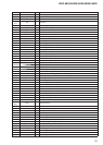
AD1 NC - Not used
AD2 BT_DET I Bluetooth signal detection signal input terminal
AD3 XNC_KEY I Key input terminal Not used