


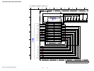
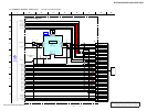

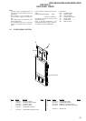

NWZ-A826/A826K/A828/A828K/A829
38
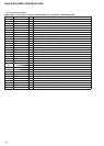
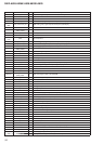
Pin No. Pin Name I/O Description
M9 NAND_CEZ0 O Chip enable signal output to the NAND fl ash memory
M10 GND - Ground terminal
M17, M18 GND - Ground terminal
M19 LCD_B0 O RGB video (blue) signal output to the liquid crystal display
M22 to
M25
LCD_G0 to LCD_G3 O RGB video (green) signal output to the liquid crystal display
M26 NC - Not used
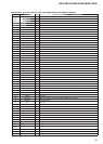
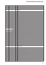
N1 to N5
SDR_DATA12 to
SDR_DATA8
I/O Two-way data bus with the SD-RAM
N8 SDR_DATA7 I/O Two-way data bus with the SD-RAM
N9, N10 GND - Ground terminal
N17 to
N19
GND - Ground terminal
N22, N23 LCD_G4, LCD_G5 O RGB video (green) signal output to the liquid crystal display
N24, N25 LCD_R0, LCD_R1 O RGB video (red) signal output to the liquid crystal display
N26 VMICIN I Power supply input terminal (+2.9 - 4.2V)
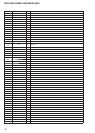
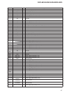
P1 to P4
SDR_DATA5 to
SDR_DATA2
I/O Two-way data bus with the SD-RAM
P5 SDR_DQM0 O Write mask signal output to the SD-RAM
P8 SDR_DATA6 I/O Two-way data bus with the SD-RAM
P9 GND - Ground terminal
P10 RESETZ O Reset signal output to the USB controller
P17 to P19 GND - Ground terminal
P22 LCD_R3 O RGB video (red) signal output to the liquid crystal display
P23 LCD_PXCLK O Pixel clock signal output to the liquid crystal display
P24 NC - Not used
P25, P26 IO_A - Not used
R1 SDR_DATA0 I/O Two-way data bus with the SD-RAM
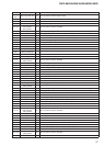
R2 to R4
SDR_DQM3 to
SDR_DQM1
O Write mask signal output to the SD-RAM
R5 SDR_WEZ O Write enable signal output to the SD-RAM
R8 SDR_DATA1 I/O Two-way data bus with the SD-RAM
R9 GND - Ground terminal
R10 NC - Not used
R17 U70_CTSZ O CTS signal output to the bluetooth controller
R18 U70_RTSZ I RTS signal input from the bluetooth controller
R19 GND - Ground terminal
R22, R23 LCD_R2, LCD_R4 O RGB video (red) signal output to the liquid crystal display
R24 GNDSINK - Ground terminal
R25 VDD_L0 I Power supply input terminal (+1.2V)
R26 NC - Not used
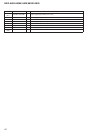
T1 SDR_CKE0 O Clock enable signal output to the SD-RAM
T2 NC - Not used
T3 SDR_CSZ0 O Chip select signal output to the SD-RAM
T4 SDR_BA1 O Bank address signal output to the SD-RAM
T5 SDR_RASZ O Row address strobe signal output to the SD-RAM
T8 NC - Not used
T9 GND - Ground terminal
T10 NC - Not used
T17 U70_SOUT O Serial data output to the WM-PORT connector and bluetooth controller
T18 U70_SRIN I Serial data input from the WM-PORT connector and bluetooth controller
T19 GND - Ground terminal
T22 LCD_R5 O RGB video (red) signal output to the liquid crystal display
T23 NC - Not used
T24 C_TMS I Mode selection signal input terminal for JTAG
T25 VLOG O Power supply output terminal (+1.8V)
T26 CKO O Main system clock output terminal (11.2896 MHz)