


NWZ-A826/A826K/A828/A828K/A829
34
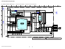
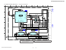
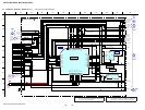
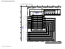
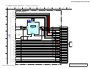
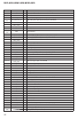
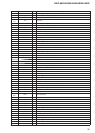
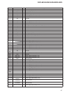
• IC Pin Function Description
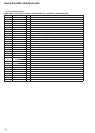
MAIN BOARD IC302 CS43L21-CNZR (A/D CONVERTER, D/A CONVERTER, HEADPHONE AMP)
Pin No. Pin Name I/O Description
1 LRCK O L/R sampling clock signal output to the system controller
2 SDA/CDIN I Serial data input from the system controller
3 SCL/CCLK I Serial data transfer clock signal input from the system controller
4 AD0/nCS I Chip select signal input from the system controller
5 VA_HP - Power supply terminal (+1.8V)
6 FLYP I External charge pump capacitor (positive node) connection terminal
7 GND_HP - Ground terminal
8 FLYN I External charge pump capacitor (negative node) connection terminal
9 VSS_HP O Negative voltage from charge pump output terminal
10 AOUTB O Analog audio (R-ch) signal output to the headphone and WM-PORT connector
11 AOUTA O Analog audio (L-ch) signal output to the headphone and WM-PORT connector
12 VA - Power supply terminal (+1.8V)
13 AGND - Ground terminal
14 DAC_FILT+ O Positive reference voltage output terminal
15 VQ O Quiescent voltage output terminal
16 ADC_FILT+ O Positive reference voltage output terminal
17 MICIN1/AIN3A I Microphone signal input terminal Not used
18 MICIN2/AIN3B/BIAS I Microphone signal input terminal Not used
19 AIN2A I Analog audio (L-ch) signal input terminal Not used
20 AIN2B/BIAS I Analog audio (R-ch) signal input terminal Not used
21, 22 AFILTA, AFILTB O Filter connection terminal Not used
23 AIN1A I Analog audio (L-ch) signal input terminal Not used
24 AIN1B I Analog audio (R-ch) signal input terminal Not used
25 nRESET I Reset signal input from the system controller
26 VL - Power supply terminal (+2.9V)
27 VD - Power supply terminal (+1.8V)
28 DGND - Ground terminal
29 SDOUT O Serial audio data output to the system controller
30 MCLK I Master clock signal input from the system controller
31 SCLK O Bit clock signal output to the system controller
32 SDIN I Serial audio data input from the system controller
33 AGND - Ground terminal