


- 43 -
Copyright © 2010 LG Electronics. Inc. All right reserved.
Only for training and service purposes
LGE Internal Use Only
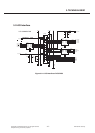
3. TECHNICAL BRIEF
ͽͶ͑ͺΟΥΖΣΟΒΝ͑ΆΤΖ͑ΟΝΪ
42/133
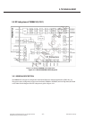
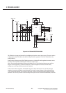
3. TECHNICAL BRIEF
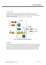
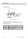
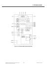
In continuous-burst mode, a data Read can traverse partition boundaries.
Upon initial power-up or return from reset, the device defaults to asynchronous arrayread mode.
Synchronous burst-mode reads are enabled by programming the Read Configuration Register. In
synchronous burst mode, output data is synchronized with a user-supplied clock signal. A WAIT
signal provides easy CPU-to-flash memory synchronization.
Designed for low-voltage applications, the device supports read operations with VCC at 1.8 V, and
erase and program operations with VPP at 1.8 V or 9.0 V. VCC and VPP can be tied together for a
simple, ultra-low power design. In addition to voltage flexibility, a dedicated VPP connection
provides complete data protection when VPP is less than VPPLK.
A Status Register provides status and error conditions of erase and program operations.
One-Time-Programmable (OTP) registers allow unique flash device identification that can be used to
increase flash content security. Also, the individual block-lock feature provides zero-latency block
locking and unlocking to protect against unwanted program or erase of the array.
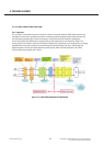
The flash memory device offers three power savings features:
• Automatic Power Savings (APS) mode: The device automatically enters APS following a read-cycle
completion.
• Standby mode: Standby is initiated when the system deselects the device by deasserting CE#.
• Deep Power-Down (DPD) mode: DPD provides the lowest power consumption and is enabled by
programming in the Enhanced Configuration Register. DPD is initiatied by asserting the DPD pin.
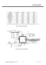
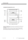
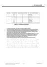
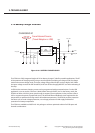
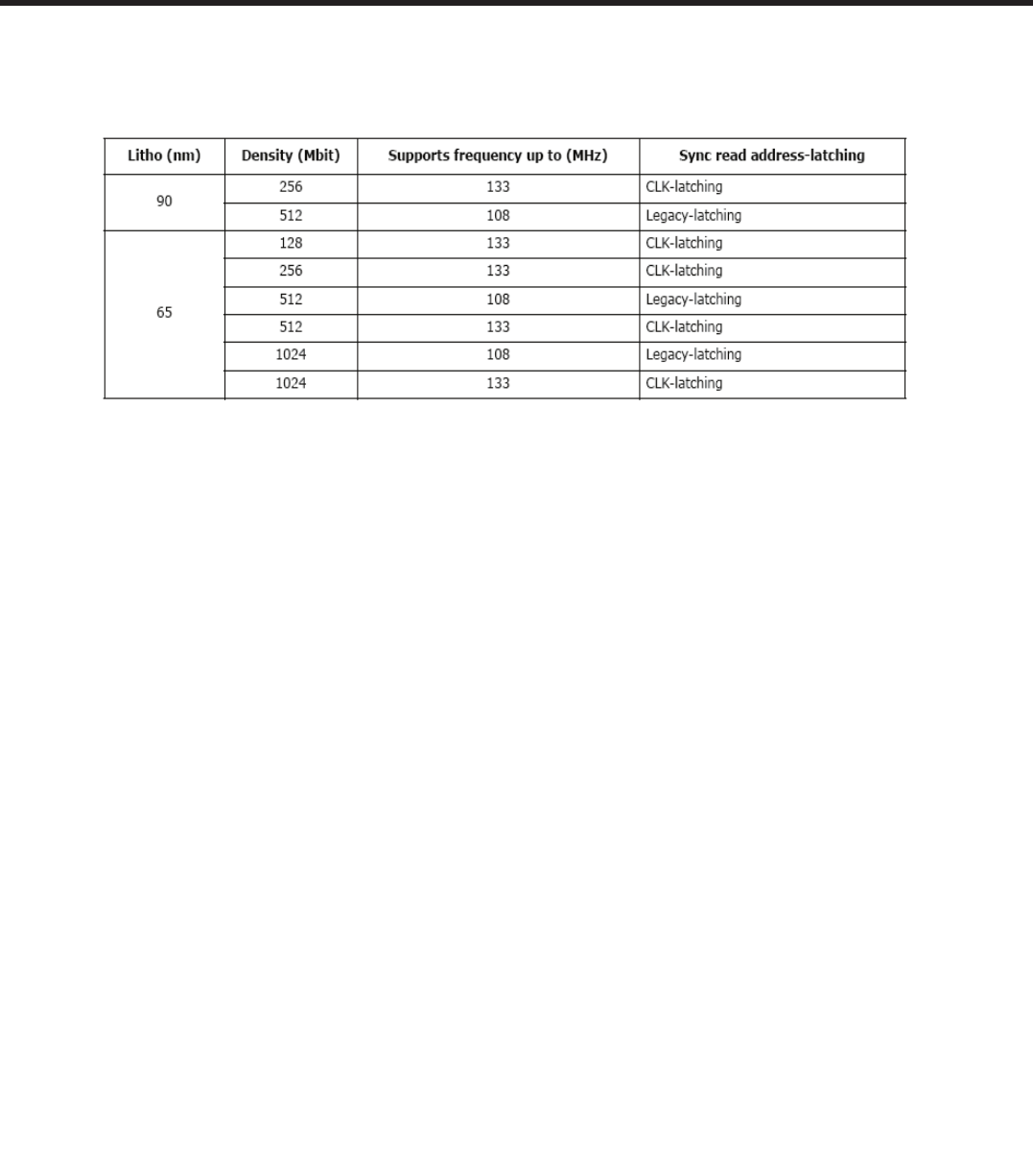
Table 3_6_1 M18 Frequency combinations