


- 45 -
Copyright © 2010 LG Electronics. Inc. All right reserved.
Only for training and service purposes
LGE Internal Use Only
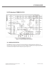
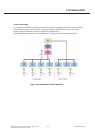
3. TECHNICAL BRIEF
ͽͶ͑ͺΟΥΖΣΟΒΝ͑ΆΤΖ͑ΟΝΪ
[[VXZZ
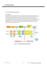
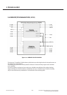
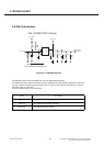
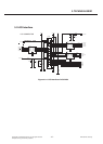
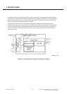
3.7.1 Transmitter path
3. TECHNICAL BRIEF
This module features a fully integrated zero IF transmitter. The baseband transmitted data Is digitally
modulated in the modem block and up-converted the 2.4GHz ISM band in the Transmitter path. The
transmitter path consists of signal filtering, I/Q up-conversion, high -output power amplifier(PA), and
RF filtering. It also incorporates modulation schemes P/4-DQPSK for 2 Mbps and 8-DPSK for 3 Mbps to
support enhanced data rate.
• Digital modulator
The digital modulator performs the data modulation and filtering required for the GFSK, b/4DQPSK,
and 8-DPSK signal. The fully digital modulator minimizes any frequency drift or anomalies in the
modulation characteristics of the transmitted signal and is much more Stable than direct VCO
modulation schemes.
• Power Amplifier
The integrated PA for the BCM2070 is configurable for Class 2 operation, transmitting up to +4 dBm as
well as Class 1 operation and transmit power up to +12 dBm at the chip, gFSK, >2.5V supply. Due to
the linear nature of the PA, combined with some integrated filtering, no External filters are requires for
meeting Bluetooth and regulatory harmonic and spurious requirements. For integrated mobile
handset applications, where Bluetooth is integrated next to the celluar radio, minimal external filtering
can be applied to achieve near thermal noise levels for spurious and radiated noise emissions.
Using a highly linearized, temperature compensated design the PA can transmit +12 dBm for Basic rate
and +10 dBm for enhanced data rates(2 to 3 Mbps). A flexible supply voltage range Allows the PA to
operate from 1.2V to 3.0V. The minimum supply voltage at VDDTF is 1.8V to achieve +10dBm of
transmit power.
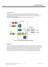
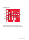
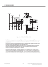
3.7.2 Receiver path
The receiver path uses a low IF scheme to down-convert the received signal for demodulation in the
digital demodulator and bit synchronizer. The receiver path provides a high degree of Linearity, an
extended dynamic range, and high order on-chip channel filtering to ensure reliable operation in the
noisy 2.4GHz ISM bnad. The front-end topology, with built-in out -of-bnad attenuation, enables the
device to be used in most applications with no off-chip Filtering. For integrated handset operation
where the Bluetooth function is integrated close to the celluar transmitter, minimal external filtering is
required to eliminate the desensitization of The receiver by the cellular transmit signal.