


- 29 -
Copyright © 2010 LG Electronics. Inc. All right reserved.
Only for training and service purposes
LGE Internal Use Only
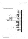
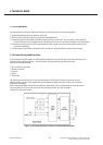
3. TECHNICAL BRIEF
3.2.2 Output voltage regulation
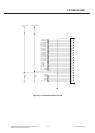
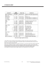
The QSC62x0 device includes all the regulated voltages needed for most low-cost wireless
handset applications (and many other applications). Independent regulated power sources are
required for various electronic functions to avoid signal corruption between diverse circuits,
support power-management sequencing, and meet different voltage-level requirements. Sixteen
voltage regulators are provided — all programmable, all derived from a common bandgap reference circuit.
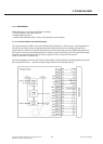
Three major types of voltage regulator circuits are on-chip:
Three positive voltage switched-mode power supply (SMPS) circuits
- One boost converter (rated for 600 mA)
- Three buck converters (rated for 500 mA each)
Thirteen positive voltage linear regulators
- Four rated for 300 mA
- Six rated for 150 mA
- Three rated for 50 mA
One negative voltage charge pump rated for 200 mA, referred to as a negative charge pump(NCP)
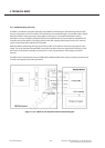
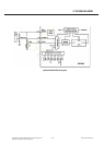
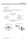
Each regulator has two logic-OR input bits; a logic high at either input enables that regulator:
A master bit that enables all regulators according to their default condition
A dedicated bit that enables only that regulator
The master enable reduces the number of write cycles needed when switching between the phone’s
sleep and active modes.
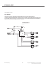
Additional comments that apply to regulator functions:
If a regulator’s default condition is on, that regulator will power on automatically at QSC startup.
The MSMP regulator must be on to allow internal communications between major functional blocks.
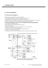
Each regulator and SMPS can provide more than its rated output current, though some
performance characteristics might be degraded.
All regulated output voltages are programmable.
All regulators can be set to a low-power mode except the VREG_USB_3P3 and VREG_NCP circuits