


- 43 -
Copyright © 2010 LG Electronics. Inc. All right reserved.
Only for training and service purposes
LGE Internal Use Only
3. TECHNICAL BRIEF
G
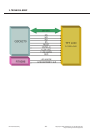
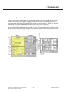
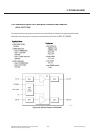
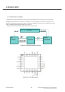
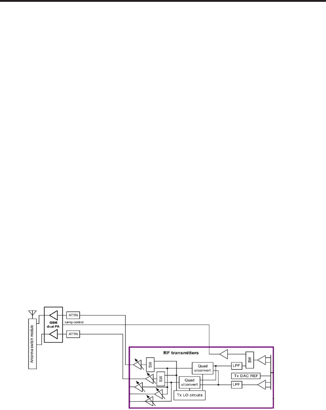
3.5.2 GSM TRANSMITTER
The RF transmitters are leveraged from previous-generation RTR™ devices, including the latest innovations.
The ESC transmitter paths and Tx power-detector input are discussed in this section. It provides the zero-IF
(ZIF) transmit signal paths for multiband, multimode applications:
Quad-band GSM:
Low-band
GSM 850 (869 to 894 MHz) and GSM 900 (925 to 960 MHz)
High-band
DCS1800 (1805 to 1880 MHz) and PCS1900 (1930 to 1990 MHz)
The transmit signal paths include a shared set of baseband amplifiers, a dedicated quadrature upconversion
for each band-type (low and high), gain control RF amplification, and multiple output driver amplifiers for
each band-type. Two GSM output drivers support one low-band and one high-band type (but each GSM
band-type is dual-band). The GSM transmitters in polar PA configuration are also supported by a PA envelope
control path, plus the ability to route LO signals to the transmit chains for test and calibration purposes. In
linear PA configuration, phase and envelope paths are combined inside the ESC and amplified using a
multistage linear PA.
Numerous secondary Tx functions are also integrated: a reference for the transmit DACs, the Tx phase-locked
loop (PLL), the Tx OSC circuit, the Tx LO generation and distribution circuits, an RMS Tx power detector, and
various interface, control, and status circuits.
The RF transmitter interfaces internally with the baseband circuits for its analog baseband input and status
and control signaling. Power reduction features controlled by baseband circuits (such as selective circuit
powerdown, gain control, and transmit puncturing) extend handset talk time. The driver amplifier outputs
are routed externally to the final stages of the transmit chains, culminating with the antenna switch whose
output drives the antenna.
Sophisticated Tx LO circuits implement the frequency plan and are completely integrated on-chip. All Tx LO
signals are generated by the on-chip Tx OSC under the control of its PLL.
[Figure 3.5.2] QSC GSM transmitter signal paths functional diagram