


- 42 -
LGE Internal Use Only Copyright © 2010 LG Electronics. Inc. All right reserved.
Only for training and service purposes
3. TECHNICAL BRIEF
G
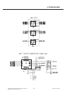
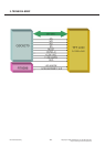
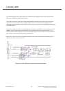
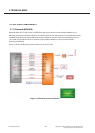
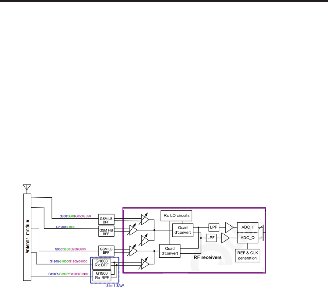
The second downconverter accepts inputs from another two LNAs (again, just one is active at time) and is
dedicated to GSM 900 and GSM 1800 operation.
The two downconverter outputs drive analog baseband filters and buffer circuits that are programmed to
support the active operating mode’s waveforms (GSM or EDGE). The analog baseband signals are then
digitized by analog-to-digital converters (ADCs) whose outputs are routed to the digital baseband circuits for
further processing.
Numerous secondary Rx functions are also integrated: Rx frequency synthesizers (each having their own PLL
and VCO circuits), LO generation and distribution circuits, reference and clock circuits for the ADCs, and
various interface, control, and status circuits. Power reduction features (such as selective circuit powerdown,
gain control, and bias control) extend handset standby time.
Like the Tx LO, all Rx LO circuits are completely integrated. All received LO signals are generated by the on-
chip Rx VCOs under control of their PLLs.
[Figure 3.5.1] QSC GSM receiver signal paths functional diagram