


Chapter 1 Overview
13
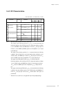
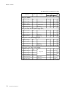
Electrical Characteristics
1-5 Electrical Characteristics
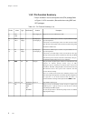
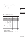
1-5-1 Absolute Maximum Ratings
∗2 ∗3
Note:
∗1
Applicable even for an interval of 100ms.
*2
Insert at least one bypass capacitor of 0.1
µ
F or more between a power source pin
and GND to prevent from latchup.
*3
Absolute maximum ratings indicate the allowable limit to which applied voltage
does not damage a chip, not guarantee the operation.
This LSI manual describes
standard specifications.
Before using the LSI, please
obtain product specifications
from the sales office.
Contents
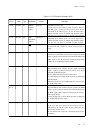
Model
MN101C117/115
Classification CMOS integrated circuit
Use General purpose
Function CMOS, 8-bit, single-chip microcomputer
Parameter Symbol Rating Unit
1 Supply voltage V
DD
–0.3
to
+7.0 V
2 Input clamp current (SENS) IC –500
to
500 µA
3 Input pin voltage V
I
–0.3
to
V
DD
+0.3 V
4 Output pin voltage V
O
–0.3
to
V
DD
+0.3 V
5 I/O pin voltage V
IO1
–0.3
to
V
DD
+0.3 V
6
Peak output
I
OL1
(peak)
7
current
I
OL2
(peak)
8I
OH
(peak)
mA
9
Average output
I
OL1
(avg)
10
current
*1
I
OL2
(avg)
11 I
OH
(avg)
12 Tolerable loss PD mW
13
Ambient operating temperature
T
opr
°C
14 Storage temperature T
stg
°C
30
20
–10
20
15
–5
400
–40
to
85
–55
to
+125
P8
Except P8
All pins
P8
Other than P8
All pins