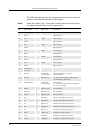
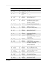
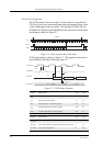
Your Privacy
When you visit our website, we store cookies on your browser to collect information. The information collected might relate to you, your preferences or your device, and is mostly used to make the site work as you expect it to and to provide a more tailored web experience. However, you can choose not to allow certain types of cookies, which may impact your experience of the site and the services we are able to offer. Click on the different category headings to find out more and change our default settings according to your preference. You cannot opt-out of our First Party Strictly Necessary Cookies as they are deployed in order to ensure the proper functioning of our website (such as prompting this preference center and remembering your settings, to log into your account, to redirect you when you log out, etc.). For more information about the First and Third Party Cookies used please follow this link. More information