


I - 3
Chapter 1 Overview
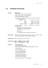
Hardware Functions
1-2 Hardware Functions
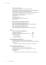
CPU Core MN101C Core
- LOAD-STORE architecture (3-stage pipeline)
- Half-byte instruction set / Handy addressing
- Memory addressing space is 256 KB
- Minimum instructions execution time (3.0 V to 3.6 V for Flash version)
High speed oscillation
[normal] 0.10 µs / 20 MHz (2.5 V to 3.6 V)
0.20 µs / 10 MHz (2.1 V to 3.6 V)
0.50 µs / 4 MHz (1.8 V to 3.6 V)
[2x-speed] 0.119 µs / 8.39 MHz (2.5 V to 3.6 V)
Low speed oscillation 61.04 µs / 32.768 kHz (1.8 V to 3.6 V)
- Operation modes
NORMAL mode ( High speed oscillation )
SLOW mode ( Low speed oscillation )
HALT mode
STOP mode
(The operation clock can be switched in each mode.)
Memory bank Data memory space expansion by bank form (4 banks unit : 64 KB / 1 bank)
- Bank for source address / Bank for destination address
ROM correction Max.3 parts in program can be corrected
Internal memory ROM 48 KB (Flash version 128 KB)
RAM 3 KB (Flash version 6 KB)
Interrupts 17 Internal interrupts
<Non-maskable interrupt (NMI)>
- Incorrect code execution interrupt and Watchdog timer interrupt
< Timer interrupts >
- Timer 0 interrupt (8-bit timer)
- Timer 1 interrupt (8-bit timer)
- Timer 4 interrupt (8-bit timer)
- Timer 5 interrupt (8-bit timer)
- Timer 6 interrupt (8-bit timer)
- Time base interrupt (8-bit timer)
- Timer 7 interrupt (16-bit timer)
- Match interrupt for Timer 7 compare register 2