


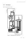
Chapter 8 Time Base Timer / 8-bit Free-running Timer
VIII - 6
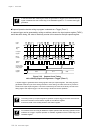
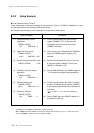
Control Registers
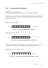
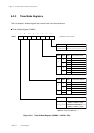
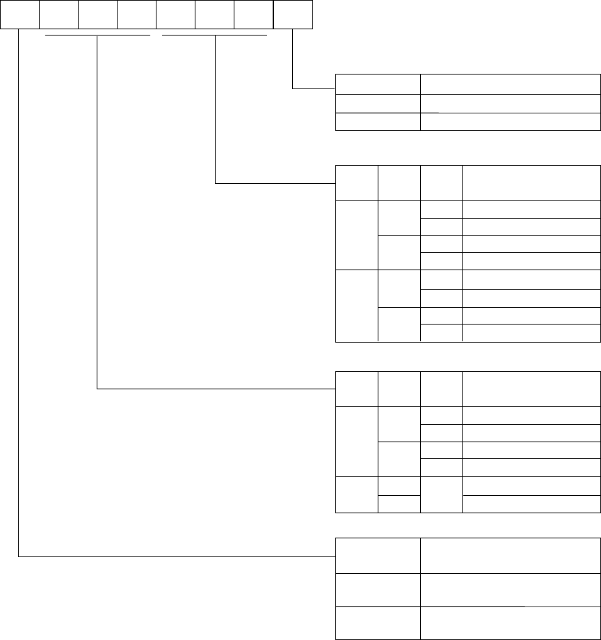
TM6CK3
0
TM6CK2
0
1
0
1
1
fs
fx
Timer 6 clock source
fosc
0
0
1
1
0
1
TM6CK1
01
24
567
3
( At reset : 0 0 0 0 0 0 0 0 )
TM6MD
TM6CK0TM6CK1
TM6CK2TM6CK3TM6IR0
TM6IR1TM6IR2
TM6CLRS
0
1
TM6CLRS
0
1
0
1
fosc
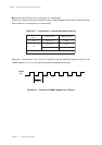
Time base timer clock source
fx
TM6CKS0
Synchronous fx
Synchronous time base selection clock ×
1/2
Time base selection clock × 1/2
Time base selection clock ×1/2
Synchronous time base selection clock ×
1/2
TM6IR2
0
TM6IR1
0
1
0
1
1
0
0
1
1
TM6IR0
-
Time base selection clock × 1/2
Time base timer
interrupt cycle selection
Enable the initialization of
TM6BC as TM6OC is written
Disable the initialization of
TM6BC as TM6OC is written
Timer 6 binary counter clear
7
13
12
13
12
Time base selection clock × 1/2
8
Time base selection clock × 1/2
9
Time base selection clock × 1/2
10
Time base selection clock × 1/2
13
Time base selection clock × 1/2
15
* TM6IRQ is disabled as TM6CLRS = 0,
TM6IRQ is enabled as TM6CLRS = 1.
Figure 8-2-4 Timer 6 Mode Register (TM6MD : x'03F6A', R/W)
8-2-3 Timer Mode Registers
This is a readable / writable register that controls timer 6 and time base timer.
Timer 6 Mode Register (TM6MD)