


Chapter 2 CPU Basics
II - 4
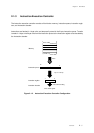
Overview
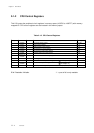
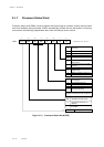
2-1-2 CPU Control Registers
This LSI locates the peripheral circuit registers in memory space (x'03F00' to x'03FFF') with memory-
mapped I/O. CPU control registers are also located in this memory space.
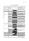
Table 2-1-2 CPU Control Registers
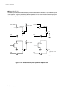
[ Chapter 3 ]
[ Chapter 3 ]
R/W : Readable / Writable *1 a part of bit is only readable
Registers Address R/W Function Pages
CPUM
x'03F00'
R/W *1
CPU mode control register II - 21,25
MEMCTR
x'03F01'
R/W
Memory control register II - 16
RCCTR
x'03F0E'
R/W
ROM correction control register II - 32
SBNKR
x'03F0A'
R/W
Bank register for source address II - 28
DBNKR
x'03F0B'
R/W
Bank register for destination address II - 28
OSCMD
x'03F2D'
R/W
Oscillation frequency control register II - 25
RCnAP
x'03FC7' to
x'03FCF'
R/W ROM correction address setting register II - 33, 34
Reserved
x'03FE0'
-
For debugger -
NMICR
x'03FE1'
R/W
Non - maskable interrupt control register III - 16
xxxICR
x'03FE2' to
x'03FFE'
R/W Maskable interrupt control register III - 17 to 37
Reserved
x'03FFF'
-
Reserved ( For reading interrupt vector data on interrupt process) -