Operation
Chapter 14 Automatic Transfer Controller
XIV - 9
13
14-3 Operation
14-3-1 Basic Operations and Timing
ATC1 is a DMA block that enables the hardware to transfer the whole memory space (256 KB). This section
provides a description of and timing for the basic ATC1 operations.
ATC1 activation and internal bus acquisition
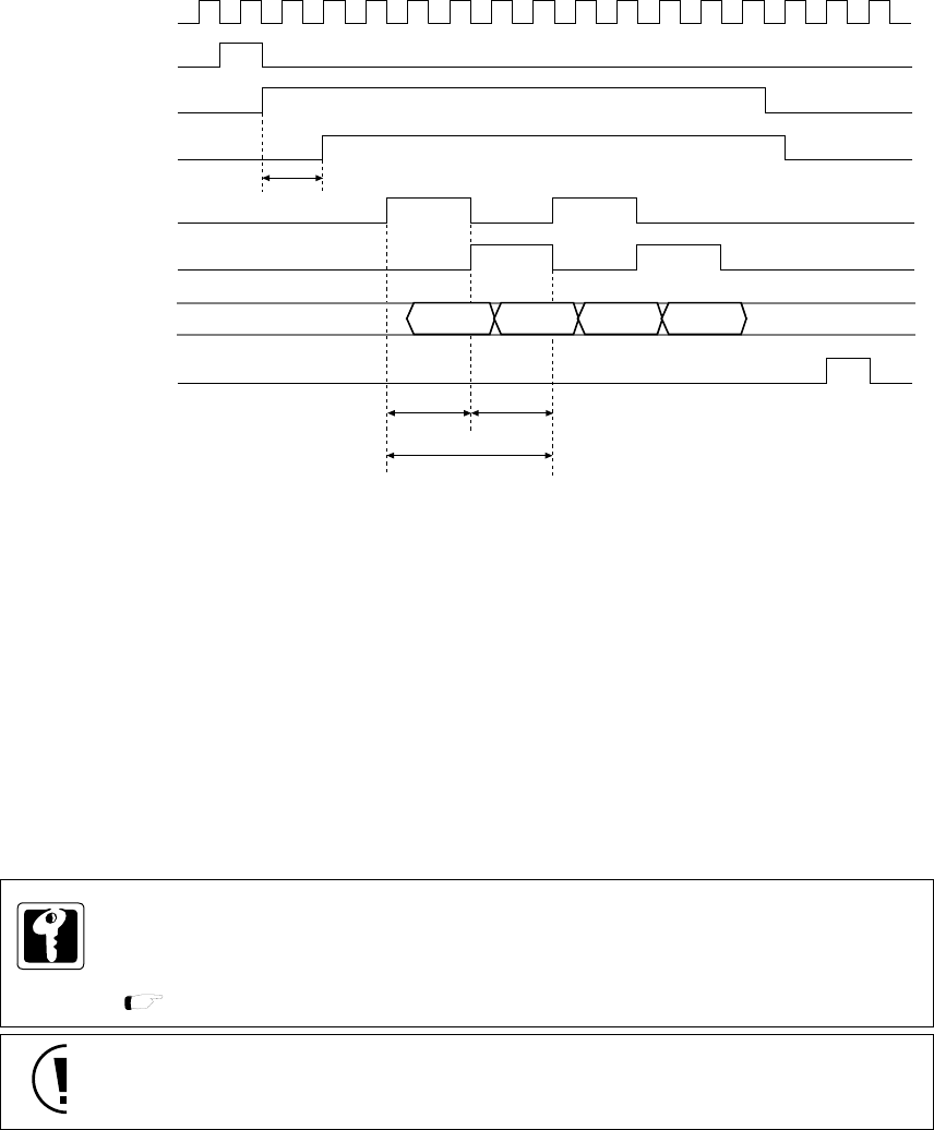
ATC1 activates either when the selected interrupt factor occurs or when the software sets the activation
flag. Set the ATC1 trigger factor in ATC1 control register 1 (AT1CNT1).
When ATC1 starts, the ATC1 controller asserts the BREQ signal, which requests the MCU core to
release the bus. When the core receives the BREQ signal, it stops all normal executions, even if it is in
the middle of executing an instruction, and releases the bus at the next available timing. The core takes
a maximum of four cycles from the time it receives the BREQ signal until it actually releases the bus.
After it releases the internal bus, the core returns the bus granted signal, BGRNT, to ATC1. ATC1 can
then begin using the bus to transfer data.
When an external interrupt is selected as an ATC1 trigger factor, specify the activa-
tion valid edge by the REDGn flag of the external interrupt control register, and the
EDGSELn flag of the both edges interrupt control register (EDGDT).
[ Chapter 3 3-3. External interrupts]
Figure 14-3-1 ATC1 Timing Chart
System clock (fs)
BREQ
BGRNT
LDDMA
STDMA
ATC1IRQ
Address bus
DMA start request
(synchronous signal)
Source source
Destination destination
Load cycle
Byte data transfer cycle
Store cycle
CPU bus release adjustment cycle
Set the valid edge for external interrupts before ATC1 activates.


