


II - 37
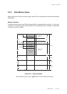
Chapter 2 CPU Basics
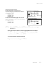
ROM Correction
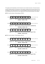
108FC
108FD
108FF
10900
10901_
85
A011
58
EC1
A081
Address
Data
The second program to be corrected (internal ROM)
sub d1, d1
mov 11, d0
mov d0, (a0)
addw 1, a0
mov _Msyscom_edge, 0
The head address of the correction
(the set value of RC1AP)
The address for recover
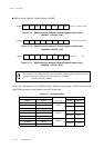
006BC
006BE
006BF
A041
58
3920090
Address
Data
The second correct program (internal RAM)
mov 14, d0
mov d0, (a0)
jmp 10900
The head address of the correction program
(the set value of RC1V)
The address for recover
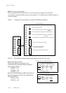
[Setup for the second correction]
Set the head address of the program to be
corrected at second to the ROM correction address 1
setting register (RC1AP).
RC1APL = x'FD'
RC1APM = x'08'
RC1APH = x'01'
Set the internal RAM address x'06BC' that stored the
second correct program to the RC vector table address
(RC1V(L), RC1V(H).
RC1V(L) = x'BC'
RC1V(H) = x'06'
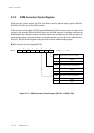
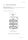
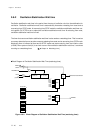
(STEP 3) Set the bit 0 (RC0EN) and the bit 1 (RC1EN) of the ROM correction control register
(RCCTR) to "1".
After the main program is started, the instruction fetched address and the set address
to the ROM correction address setting register (RCnAP) are always compared, then
once they are matched program counter indirectly branches to the address in RAM
area, that are stored to the RC vector table (RCnV).
The correction program in RAM area is executed.
Program counter recovers to the program in ROM area.