XVIII - 13
Chapter 18 Flash EEPROM
Onboard Serial Interface Programming Mode
18-6-2 Circuit Requirements for the Target Board
(in Clock Synchronous Communication using the YDC Serial
Writer)
This section describes the circuit requirements for the target board for onboard serial programming with
the serial interface 0 using YDC serial writer.
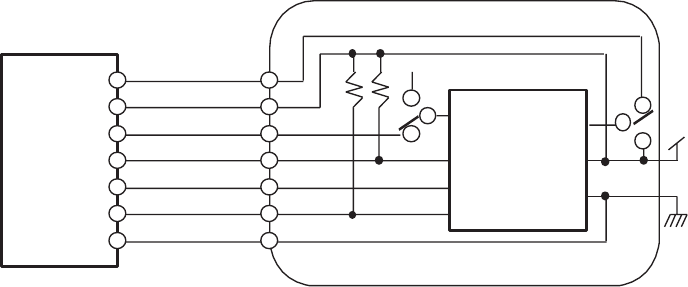
Figure 18-6-1 Target Board for programming using the YDC Serial Writer
Pins
VPP : 5.0 V power supply (for Flash EEPROM)
VDD : MN101CF77G: 2.7 V to 3.6 V power supply (for Flash EEPROM and internal circuits)
NRST : Reset
P03 : Serial interface 0 data I/O pin (used as SBO0 pin as well)
P05 : Serial interface 0 clock pin (used as SBT0 pin as well)
P04 : Busy signal output pin (used as SBI0 as well)
VSS : Ground
YDC
Serial
Writer
VPP
VDD
VSS
MN101CF77G
P04
P05
P03
NRST
VDD
P05
NRST
P04
P03
VPP
VSS
Target Board


