


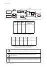
Chapter 2 CPU Basics
II - 34
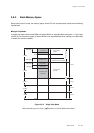
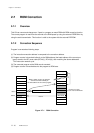
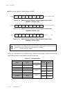
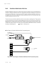
ROM Correction
Here is the correspondence of the ROM correction address setting register, a ROM correction control
flag of ROM correction control register and the RC rector table.
Table 2-7-1 Correspondence
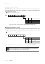
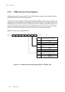
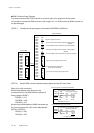
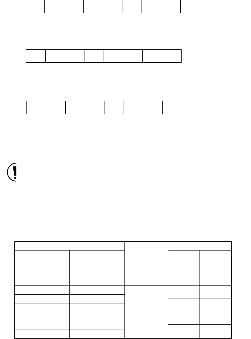
ROM Correction Address 2 Setting Register (RC2AP)
Figure 2-7-9 ROM Correction Address 2 Setting Register (lower 8 bits)
(RC2APL : x'03FCD', R/W)
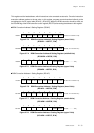
Figure 2-7-10 ROM Correction Address 2 Setting Register (middle 8 bits)
(RC2APM : x'03FCE', R/W)
Figure 2-7-11 ROM Correction Address 2 Setting Register (upper 2 bits)
(RC2APH : x'03FCF', R/W)
RC2APL7
76543210
RC2APL6 RC2APL5 RC2APL4 RC2APL3 RC2APL2 RC2APL1 RC2APL0
( At reset : X X X X X X X X)
RC2APL
RC2APM7
76543210
RC2APM6RC2APM5RC2APM4RC2APM3RC2APM2RC2APM1RC2APM0
( At reset : X X X X X X X X )
RC2APM
-
76543210
-----RC2APH1 RC2APH0
( At reset : - - - - - - X X )
RC2APH
Do not set the same address to more than two RCnAP (H/M/L) register. If there are several
registers set the same address, the order of priority is as follows :
RC0AP > RC1AP > RC2AP
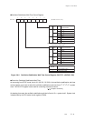
ROM correction
Register Address control flag Vector Address
RC0APL x'3FC7' RC0V(L) x'0010'
RC0APM x'3FC8'
RC0APH x'3FC9'
RC1APL x'3FCA' RC1V(L) x'0014'
RC1APM x'3FCB'
RC1APH x'3FCC'
RC2APL x'3FCD' RC2V(L) x'0013'
RC2APM x'3FCE'
RC2APH x'3FCF'
RC2V(H) x'0015'
RC-vector table
RC0V(H) x'0012'
RC1V(H) x'0011'
ROM Correction address setting register
RC0EN
RC1EN
RC2EN