


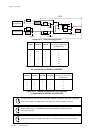

Chapter 2 CPU Basics
II - 26
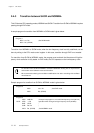
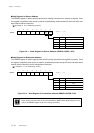
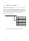
Clock Switching
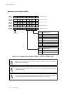
Figure 2-5-3 Clock Switching Circuit
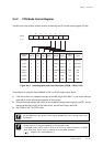
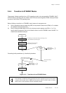
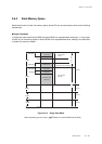
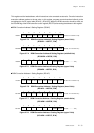
Figure 2-5-4 Setting Division Factor at NORMAL mode
by combination of OSCSEL and OSCDBL
Figure 2-5-5 Setting Division Factor at SLOW mode
by combination of OSCSEL and SOSC2DS
On clock switching, set each flag of OSCDBL, OSCSEL, SOSCSEL and OSC0, individually.
Even if those flags are mapped on the same special functions register, set twice.
0
0
00
01
1*
11
11
1
1
OSCSEL[1:0]
OSCDBL
OSC0
SOSC2DS
CPU
1
0
System Clock
4
2
2
4
16
2
fosc
fx
fs
0
1
SOSCDBL
.
.
.
.
.
.
.
High-frequency
Low-frequency
Set the OSC0 flag to "0" (NORMAL mode) before switching of division factor for
low-frequency input.
Set the division factor in SLOW mode only to 1 to 4 division and do not set other values.
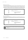
Division factor for
High-frequency (OSC) Input
(NORMAL mode)
000 2
001 1
010 8
011 4
100 32
101 16
110 64
111 64
OSCSEL1 OSCSEL0 OSCDBL
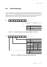
Division factor for
Low-frequency (XI / XO) Input
(SLOW mode)
0000 2
0001 4
0010 1
0011 2
0110 4
OSCSEL1 OSCSEL0 SOSCDBL SOSC2DS