


II - 33
Chapter 2 CPU Basics
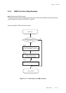
ROM Correction
This register set the head address, which instructions to be corrected are stored to. Once the instruction
execution address reaches to the set value to this register, program counter branches indirectly to the
set address to the RC vector table (RCnV(L), RCnV(H)). When the ROM correction should be valid, set
the RCnEN flag of the ROM correction control register (RCCTR) after setting the address to this register.
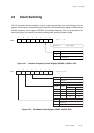
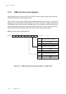
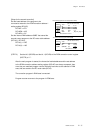
ROM Correction Address 1 Setting Register (RC1AP)
ROM Correction Address 0 Setting Register (RC0AP)
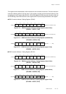
Figure 2-7-3 ROM Correction Address 0 Setting Register (lower 8 bits)
(RC0APL : x'03FC7', R/W)
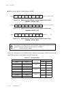
Figure 2-7-4 ROM Correction Address 0 Setting Register (middle 8 bits)
(RC0APM : x'03FC8', R/W)
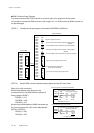
Figure 2-7-5 ROM Correction Address 0 Setting Register (upper 2 bits)
(RC0APH : x'03FC9', R/W)
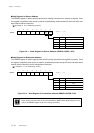
RC0APL7
76543210
RC0APL6 RC0APL5 RC0APL4 RC0APL3 RC0APL2 RC0APL1 RC0APL0
( At reset : X X X X X X X X)
RC0APL
RC0APM7
76543210
RC0APM6RC0APM5RC0APM4RC0APM3RC0APM2RC0APM1RC0APM0
( At reset : X X X X X X X X )
RC0APM
-
76543210
-----RC0APH1 RC0APH0
( At reset : - - - - - - X X )
RC0APH
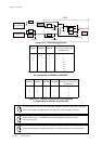
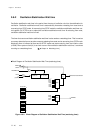
Figure 2-7-6 ROM Correction Address 1 Setting Register (lower 8 bits)
(RC1APL : x'03FCA', R/W)
Figure 2-7-7 ROM Correction Address 1 Setting Register (middle 8 bits)
(RC1APM : x'03FCB', R/W)
Figure 2-7-8 ROM Correction Address 1 Setting Register (upper 2 bits)
(RC1APH : x'03FCC', R/W)
RC1APL7
76543210
RC1APL6 RC1APL5 RC1APL4 RC1APL3 RC1APL2 RC1APL1 RC1APL0
( At reset : X X X X X X X X)
RC1APL
RC1APM7
76543210
RC1APM6 RC1APM5 RC1APM4 RC1APM3 RC1APM2 RC1APM1 RC1APM0
( At reset : X X X X X X X X )
RC1APM
-
76543210
-----RC1APH1 RC1APH0
( At reset : - - - - - - X X )
RC1APH