


Chapter 15 A/D Converter
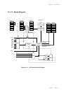
Operation
XV - 10
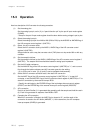
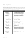
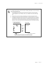
Sampling Time (Ts) of A/D Converter Setup
The sampling time of A/D converter is set by the ANSH1 to 0 flag of the ANCTR0 register. The sampling
time of A/D converter depends on external circuit, so set the right value by analog input impedance.
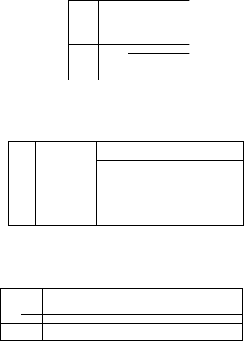
Table 15-3-3 Sampling Time of A/D Conversion and A/D Conversion Time
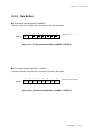
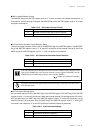
Clock of A/D Converter Setup
The A/D converter clock is set by the ANCK1 to 0 flag of the ANCTR0 register. Set the A/D converter
clock (TAD) more than 800 ns and less than 15.26 µs. Table 15-3-2 shows the machine clock (fosc, fx, fs)
and the A/D converter clock (TAD). (calculated as fs = fosc/2, fx/4)
Table 15-3-2 A/D Conversion Clock and A/D Conversion Cycle
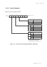
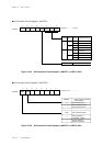
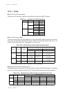
Table 15-3-1 Input Pins of A/D Converter Setup
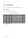
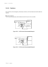
15-3-1 Setup
Input Pins of A/D Converter Setup
Input pins for A/D converter is selected by the ANCH2 to 0 flag of the ANCTR1 register.
For the system clock (fs), refer to Chapter 2. 2-5 Clock Switching.
ANCHS2 ANCHS1 ANCHS0 A/D pin
0AN0 pin
1AN1 pin
0AN2 pin
1AN3 pin
0AN4 pin
1AN5 pin
0AN6 pin
1 Reserved
0
1
0
1
0
1
at oscillation for low speed
at fosc=20 MHz at fosc=8.38 MHz at fx=32.768 kHz
200.00 ns 477.33 ns 244.14
µ
s
(no usable) (no usable ) (no usable )
400.00 ns 488.28
µ
s
(no usable) (no usable )
976.56
µ
s
(no usable )
1 fx x 2 15.26
µ
s 15.26
µ
s 15.26
µ
s
ANCK1 ANCK0
A/D
conversion
clock
at oscillation for high speed
A/D conversion cycle (TAD)
1
0
0
1
01.91
µ
s
954.65 ns
fs/2
fs/4
fs/8 800.00 ns
Sampling time
(Ts) at T
AD
=800 ns at T
AD
=954.65 ns at T
AD
=1.91
µ
sat T
AD
=15.26
µ
s
0T
AD
x 2 9.60
µ
s 11.46
µ
s 22.92
µ
s 183.12
µ
s
1T
AD
x 6 12.80
µ
s 15.27
µ
s 30.56
µ
s 244.16
µ
s
0T
AD
x 18 22.40
µ
s 26.73
µ
s 53.48
µ
s 427.28
µ
s
1Reserved - - - -
A/D conversion time
0
1
ANSH1 ANSH0