


Chapter 14 Automatic Transfer Controller
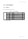
Control Registers
XIV - 8
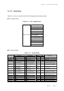
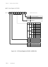
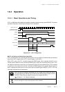
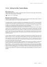
ATC1 Memory Pointer 0 (AT1MAP0)
Figure 14-2-6 ATC1 Memory Pointer 0 : Upper 2 bits (AT1MAP0H : x'03FD5', R/W)
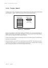
Figure 14-2-5 ATC1 Memory Pointer 0 : Middle 8 bits (AT1MAP0M : x'03FD4', R/W)
Figure 14-2-4 ATC1 Memory Pointer 0 : Lower 8 bits (AT1MAP0L : x'03FD3', R/W)
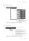
ATC1 Memory Pointer 1 (AT1MAP1)
Figure 14-2-9 ATC1 Memory Pointer 1 : Upper 2 bits (AT1MAP1H : x'03FD8', R/W)
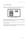
Figure 14-2-8 ATC1 Memory Pointer 1 : Middle 8 bits (AT1MAP1M : x'03FD7', R/W)
Figure 14-2-7 ATC1 Memory Pointer 1 : Lower 8 bits (AT1MAP1L : x'03FD6', R/W)
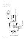
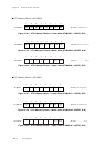
AT1MAP0L bp2 bp1 bp0bp7 bp6 bp3bp5 bp4
(At reset : x x x x x x x x )
01245673
(At reset : x x x x x x x x )
AT1MAP0M
bp10 bp9 bp8bp15 bp14 bp11bp13 bp12
01245673
(At reset : - - - - - -
x x
)
bp17 bp16
------
AT1MAP0H
01245673
(At reset :
x x x x x x x x
)
AT1MAP1L
bp2 bp1 bp0
bp7 bp6
bp3
bp5
bp4
01245673
(At reset :
x x x x x x x x
)
bp10 bp9 bp8
bp15 bp14
bp11
bp13
bp12
AT1MAP1M
01245673
(At reset : - - - - - - x x )
bp17 bp16
------
AT1MAP0H
01245673