


Chapter 2 CPU Basics
II - 18
Bus Interface
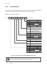
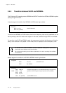
Bus Mode Control Register (CSMDn)
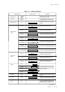
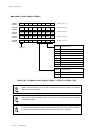
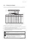
Figure 2-3-4 Bus Mode Control Register (CSMDn : x'03F05' to x'03F09', R/W)
Select 101C bus mode for the area (CS1 to CS8) where internal memory is set with the
memory area control register.
Only 101C bus mode is available in CS0 memory area, and only CSIC bus mode is available
in CS9 memory area.
For the area where CSIC bus mode is selected with the bus mode control register (CSMDn),
set always more than fixed 2 wait cycle and do not use fixed 0 or 1 wait cycle.
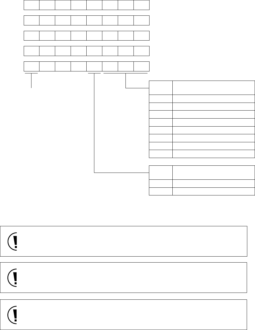
76543210
CSMD01
(X'03F05')
CS1MD CS1W2 CS1W1 CS1W0 - CS0W2 CS0W1 CS0W0
(At reset: 0110-110)
CSMD23
(X'03F06')
CS3MD CS3W2 CS3W1 CS3W0 CS2MD CS2W2 CS2W1 CS2W0
(At reset: 01100110)
CSMD45
(X'03F07')
CS5MD CS5W2 CS5W1 CS5W0 CS4MD CS4W2 CS4W1 CS4W0
(At reset: 01100110)
CSMD67
(X'03F08')
CS7MD CS7W2 CS7W1 CS7W0 CS6MD CS6W2 CS6W1 CS6W0
(At reset: 01100110)
CSMD89
(X'03F09')
RESERVED
CS9W2 CS9W1 CS9W0 CS8MD CS8W2 CS8W1 CS8W0
(At reset: 11100110)
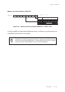
CSnW2 to 0
Wait mode selection
Set always "1"
000
001
010
011
100
101
110
111
Fixed 0 wait mode
Fixed 1 wait mode
Fixed 2 wait mode
Fixed 3 wait mode
Fixed 4 wait mode
Fixed 5 wait mode
Fixed 6 wait mode
Handshake mode
CSnMD
Bus mode selection
0
1
101C bus mode
CSIC bus mode