


XVII - 15
Chapter 17 Appendices
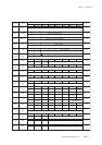
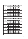
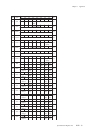
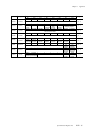
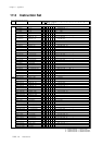
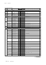
Special Function Registers List
X'3FA4'
X'3FA5'
X'3FAD'
X'3FAC'
X'3F3F' SC4ODC0
X'3F3D' SC4ODC1
X'3FF3' SC4ICR
SC4AD1
SC4TXB
SC4RXB
SC4STR
P05
Output Type
Selection
SC4 Interrupt Level Setup
Communication
Enable
Data Transmission Buffer
ACK Signal
Detection
-
-
SELI2C
I2CTXB7
I2CRXB7
WRS
SC4LV1
-
-
Reserved
I2CTXB6
I2CRXB6
I2CINT
SC4LV0
-
-
Reserved
I2CTXB5
I2CRXB5
STRT
-
-
-
I2CPSEL
I2CTXB4
I2CRXB4
RSTRT
-
-
-
I2CGEM
I2CTXB3
I2CRXB3
I2CBSY
-
-
-
I2CADM
I2CTXB2
I2CRXB2
Data Reception Buffer
SLVBSY
-
SC4ODC01
SC4ODC11
I2CAD9
I2CTXB1
I2CRXB1
ACKVALID
SC4IE
SC4ODC00
SC4ODC10
I2CAD8
I2CTXB0
I2CRXBS0
-
SC4IR
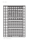
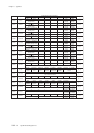
XIV - 8
XIV - 8
III - 39
XIV - 6
XIV - 5
XIV - 5
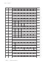
X'3FA3' SC4AD0
I2CAD7 I2CAD6 I2CAD5 I2CAD4 I2CAD3 I2CAD2
Addressing Register
I2CAD1 I2CAD0
XIV - 6
XIV - 7
Serial Interface
Pin Selection
Communication
Mode
Selection
Address
Selection
Addressing Register
Transfer
Direction
Determination
Interrupt
Detection
Bus Busy
Detection
Slave Busy
Detection
Start
Detection
Re-Start
Detection
P03
Output Type
Selection
P05
Output Type
Selection
P03
Output Type
Selection
SC4 Interrupt
Enable
SC4 Interrupt
Request
Address Register
Bit Symbol / Initial Value / Description
Bit 4 Bit 3 Bit 2 Bit 1 Bit 0
Page
Bit 7 Bit 6 Bit 5