


XI - 59
Chapter 11 Serial Interface 0, 1
Operation
Setup Procedure Description
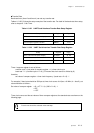
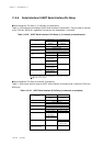
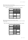
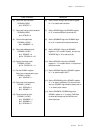
(6) Select the start condition.
SC0MD0 (x'3F92')
bp3 : SC0STE = 1
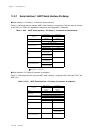
(7) Select the first bit to be transfered.
SC0MD0 (x'3F92')
bp4 : SC0DIR = 0
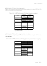
(8) Control the output data.
SC0MD2 (x'3F94')
bp0 : SC0BRKE = 0
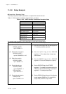
(9) Select the added parity bit.
SC0MD2 (x'3F94')
bp3 : SC0NPE = 0
bp5-4 : SC0PM1-0 = 00
(10) Specify the frame mode.
SC0MD2 (x'3F94')
bp7-6 : SC0FM1-0 = 11
(11) Set the SC0MD1 register.
Select the communication type.
SC0MD1 (x'3F93')
bp0 : SC0CMD = 1
(12) Select the clock frequency.
SC0MD1 (x'3F93')
bp3 : SC0CKM = 1
bp2 : SC0MST = 1
(13) Control the pin function.
SC0MD1 (x'3F93')
bp4 : SC0SBOS = 1
bp5 : SC0SBIS = 1
bp7 : SC0IOM = 0
(6) Set the SC0STE flag of the SC0MD0 register
to "1" to enable start condition.
(7) Set the SC0DIR flag of the SC0MD0 register
to "0" to select MSB as first transfer bit.
(8) Set the SC0BRKE flag of the SC0MD2 regis-
ter to "0" to select serial data transmission.
(9) Set the SC0PM1-0 flag of the SC0MD2
register to "00" to select 0 parity, and set the
SC0NPE flag to "0" to add parity bit.
(10) Set the SC0FM1-0 flag of the SC0MD2
register to "11" to select 8 bits + 2 stop bits at
the frame mode.
(11) Set the SC0CMD flag of the SC0MD1 register
to "1" to select duplex UART.
(12) Set the SC0CKM flag of the SC0MD1 register
to "1" to select "divided by 8" at source clock.
And, the SC0MST flag should be always set to
"1" to select colck master.
(13) Set the SC0SBOS, SC0SBIS flag of the
SC0MD1 register to "1" to set the TXD0A pin
to serial data output and the RXD0A pin to
serial data input.