Chapter 6 8-bit Timers
VI - 26
8-bit PWM Output
6-6 8-bit PWM Output
The TMnIO pin outputs the PWM waveform, which is determined by the match timing for the compare
register and the overflow timing of the binary counter.
6-6-1 Operation
Operation of 8-bit PWM Output (Timers 0, 4 and 5)
The PWM waveform with any duty cycle is generated by setting the duty cycle of PWM "H" period to the
compare register (TMnOC). The cycle is the period from the full count to the overflow of the 8-bit timer.
Table 6-6-1 shows PWM output pins ;
Ti mer 0 Ti mer 4 Timer 5
PWM output pin
TM0IO output pin
(P10, P11)
TM4IO output pin
(P12, P13)
TM5IO output pin
(P52)
Table 6-6-1 Output Pins of PWM Output
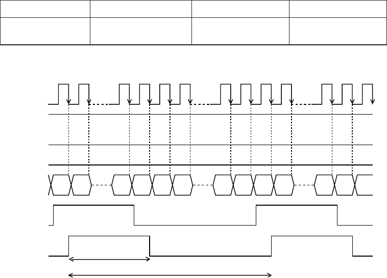
Count Timing of PWM Output (at normal) (Timers 0, 4 and 5)
Figure 6-6-1 Count Timing of PWM Output (at Normal)
PWM source waveform,
(A) is "H" while counting up from x'00' to the value stored in the compare register.
(B) is "L" after the match to the value in the compare register, then the binary counter
continues counting up till the overflow.
(C) is "H" again, if the binary counter overflow.
The PWM outputs the PWM source waveform with 1 count clock delay. This is
happened, because the waveform is created inside to correct the output cycle.
N
N+1 N+2 FE
FF
Count
clock
TMnEN
flag
Compare
register
Binary
counter
00 01 N+1N-1
N
00 01 N-1
N
TMnIO output
(PWM output)
PWM basic components ( overflow time of binary counter)
Set time in the compare register
PWM source
wave form
(A)
(B)
(C)


