


Chapter 11 Serial Interface 0, 1
XI - 36
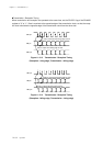
Operation
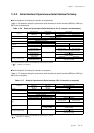
Serial Interface 1 Pins Setup (3 channels, at reception)
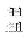
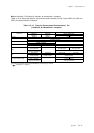
Table 11-3-12 shows the setup for synchronous serial interface pin with 3 channels (SBO1 pin, SBI1 pin,
SBT1 pin) at reception.
Table 11-3-12 Setup for Synchronous Serial Interface 1 Pin (3 channels, at reception)
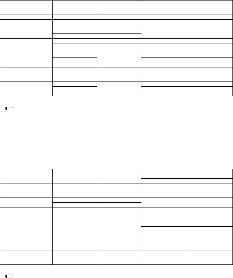
11-3-3 Serial interface 1 Synchronous Serial Interface Pin Setup
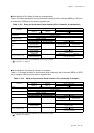
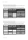
Serial Interface 1 Pins Setup (3 channels, at transmission)
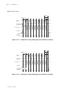
Table 11-3-11 shows the setup for synchronous serial interface pin with 3 channels (SBO1 pin, SBI1 pin,
SBT1 pin) at transmission.
Table 11-3-11 Setup for Synchronous Serial Interface 1 Pin (3 channels, at transmission)
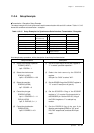
Data output pin Data input pin
SBO1A pin/ SBI1A pin/
SBO1B pin SBI1B pin Internal clock External clock
Port Pin P00/P73 P01/P74
Serial data output "1" input Serial clock I/O Serial clock I/O
SC0MD1(SC0SBOS) SC0MD1(SC0SBIS)
Push-pull / Push-pull / Push-pull /
Nch open-drain Nch open-drain Nch open-drain
SC1ODC(SC1ODC0)
SC1ODC(SC1ODC2)
Output mode Output mode Input mode
P0DIR (P0DIR0)
P7DIR (P7DIR3)
Add/Not Add Add/Not Add Add/Not Add
P0PLU (P0PLU0)
P7PLUD(P7PLUDD3)
Clock I/O pin
SBT1A pin/SBT1B pin
P02/P75
Select used pin (A, B)
SC1ODC (SC1SEL)
SBI0/SBO0 independent
SC0MD1 (SC0IOM)
Style
-
SC0MD1 (SC0SBTS)
SC1ODC (SC1ODC1)/SC1ODC (SC1ODC3)
-
Setup item
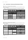
Port Pin Setup
SBI / SBO pin Setup
Function
P0DIR (P0DIR2)
P7PLUD (P7PLUD5)
Note) Select pull-up/down resistor with P7RDOWN flag of FLOAT register (x'03F2E')
[ Chapter4, 4.7.2 Register ]
-
-
P7DIR (P7DIR5)
P0PLU (P0PLU2)
I/O
Pull-up (Pull-down) setup
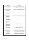
SBO0A pin/ SBI0A pin/
SBO0B pin SBI0B pin Internal clock External clock
Port Pin P03/P70 P04/P71
Port Serial data input Serial clock I/O Serial clock I/O
SC0MD1(SC0SBOS) SC0MD1(SC0SBIS)
Push-pull / Push-pull /
Nch open-drain Nch open-drain
Input mode Output mode Input mode
P0DIR (P0DIR4)
P7DIR (P7DIR1)
Add/Not Add Add/Not Add
P7PLUD (P7PLUD2)
Note) Select pull-up/down resistor with P7RDOWN flag of FLOAT register (x'03F2E')
[ Chapter4, 4.7.2 Register ]
-
-
P7DIR (P7DIR2)
P0PLU (P0PLU5)
I/O
Pull-up (Pull-down) setup
-
-
SC0MD1 (SC0SBTS)
SC0ODC (SC0ODC1)/SC0ODC (SC0ODC3)
P0DIR (P0DIR5)
Style
Setup item
Port Pin Setup
SBI / SBO pin Setup
Function
-
Clock I/O pin
SBT0A pin/SBT0B pin
P05/P72
Data input pin
Select used pin (A, B)
SC0ODC (SC0SEL)
SBI0/SBO0 independent
SC0MD1 (SC0IOM)
-