


XVIII - 15
Chapter 18 Flash EEPROM
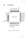
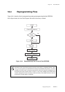
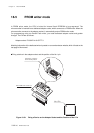
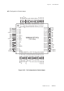
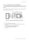
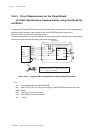
Onboard Serial Interface Programming Mode
Use of YDC serial writer
xYou must write the load program to this LSI before installed in the target board.
The load program usually comes with onboard serial writer.
xErase block 0 (load program) is write/erase-protected in the hardware during onboard
programming mode.
xVPP pin pin must supply 5.0 V from external source.
xP05, P03 and P04 pins should be reserved as dedicated pin for serial writer to prevent other
user circuits on the target board from communicating with the device. Alternatively, design your
target board on which the serial writer can program the device correctly.
xConnect pull-up resistors on the target board to P05, P03 and P04 pins, which are connected to
the power supply.
xNRST and P05 pins are output from the serial writer throgh an open connection.
xInstall a switch on the target board to toggle between NRST for serial programming and NRST
for normal opeation. Alternatively, install a wired-OR connection. (For a wired-OR connection,
disable NRST for normal operation during serial programming)
For further information of the onboard serial writer, contact :
YDC Corporation Instrument Business Division Support Center
Phone : 042-333-6245
http://www.ydc.co.jp/micom