


Chapter 17 Appendices
XVII - 14
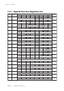
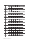
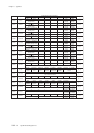
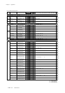
Special Function Registers List
X'3FF0'
X'3FF1'
X'3FF2'
X'3FF9'
X'3FFA'
X'3FFC'
ATC1LV1 ATC1LV0 - ATC1IE ATC1IR
ATC1ICR
Request ATC1
Interrupt
III - 37
Enable ATC1
Interrupt
Specify ATC1
Interrupt Level
TBLV1 TBLV0 - TBIE TBIR
Request TB
Interrupt
III - 27Enable TB
Interrupt
Specify TB
Interrupt Level
TBICR
TM7LV1 TM7LV0 - TM7IE TM7IR
Request TM7
Interrupt
III - 28Enable TM7
Interrupt
Specify TM7
Interrupt Level
TM7ICR
T7OC2LV1 T7OC2LV0 - T7OC2IE T7OC2IR
Request T7OC2
Interrupt
III - 29
Enable
T7OC2
Interrupt
Specify T7OC2
Interrupt Level
Specify SC0
Reception Interrupt Level
Specify SC0
Transmission Interrupt Level
Specify SC1
Reception Interrupt Level
Specify SC1
Transmission Interrupt Level
T7OC2ICR
SC3LV1 SC3LV0 - SC3IE SC3IR
SC3ICR Request SC3
Interrupt
III - 34Enable SC3
Interrupt
Specify SC3
Interrupt Level
ADLV1 ADLV0 - ADIE ADIR
ADICR Request AD
Interrupt
III - 36Enable AD
Interrupt
Specify AD
Interrupt Level
-
-
-
-
-
-
-
-
-
-
-
-
-
-
-
-
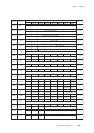
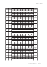
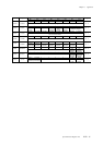
X'3FF4'
SC0RLV1 SC0RLV0 - SC0RIE SC0RIR
SC0RICR
Request SC0
Reception
Interrupt
III - 30
Enable SC0
Reception
Interrupt
---
X'3FF5'
SC0TLV1 SC0TLV0 - SC0TIE SC0TIR
SC0TICR
Request SC0
Transmission
Interrupt
III - 31
Enable SC0
Transmission
Interrupt
---
X'3FF7'
SC1TLV1 SC1TLV0 - SC1TIE SC1TIR
SC1TICR
Request SC1
Transmission
Interrupt
Enable SC1
Transmission
Interrupt
---
X'3FF6'
SC1RLV1 SC1RLV0 - SC1RIE SC1RIR
SC1RICR
Request SC1
Reception
Interrupt
III - 32
Enable SC1
Reception
Interrupt
---
III - 33
-
-
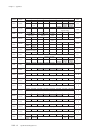
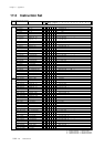
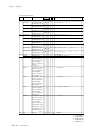
Bit 7 Bit 6 Bit 5 Bit 4 Bit 3 Bit 2 Bit 1 Bit 0
Address Register Page
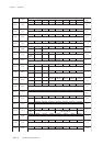
X'3FA4'
X'3FA5'
X'3FAD'
X'3FAC'
X'3F3F' SC4ODC0
X'3F3D' SC4ODC1
X'3FF3' SC4ICR
SC4AD1
SC4TXB
SC4RXB
SC4STR
P02 Output
Type Selection
SC4 Interrupt Level Setting
Enable
Communication
Operation
Data Transmission Buffer
ACK Signal
Detection
-
-
SELI2C
I2CTXB7
I2CRXB7
WRS
SC4LV1
-
-
Reserved
I2CTXB6
I2CRXB6
I2CINT
SC4LV0
-
-
Reserved
I2CTXB5
I2CRXB5
STRT
-
-
-
I2CPSEL
I2CTXB4
I2CRXB4
RSTRT
-
-
-
I2CGEM
I2CTXB3
I2CRXB3
I2CBSY
-
-
-
I2CADM
I2CTXB2
I2CRXB2
Data Reception Buffer
SLVBSY
-
SC4ODC01
SC4ODC11
I2CAD9
I2CTXB1
I2CRXB1
ACKVALID
SC4IE
SC4ODC00
SC4ODC10
I2CAD8
I2CTXB0
I2CRXBS0
-
SC4IR
XIII - 8
XIII - 8
III - 35
XIII - 6
XIII - 5
XIII - 5
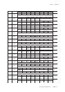
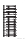
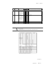
X'3FA3' SC4AD0
I2CAD7 I2CAD6 I2CAD5 I2CAD4 I2CAD3 I2CAD2
Address Setting Register
I2CAD1 I2CAD0
XIII - 6
XIII - 7
Serial Pin
Selection
Comunication
Mode Selection
Address
Setting
Selection
Address Setting
Register
Transfer
Direction
Determination
Interrupt
Detection
Bus Busy
Detection
Slave Busy
Detection
Start
Detection
Restart
Detection
P01 Output
Type Selection
P54 Otput
Type Selection
P53 Output
Type Selection
Enable SC4
Interrupt
Enable SC4
Interrupt
Set Always
to "0"
Set Always
to "0"
Bit Symbol /Initial Value /Description