


I - 13
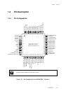
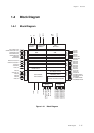
Chapter 1 Overview
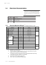
Pin Description
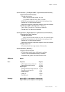
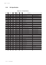
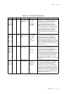
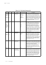
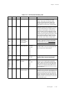
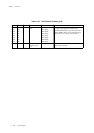
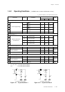
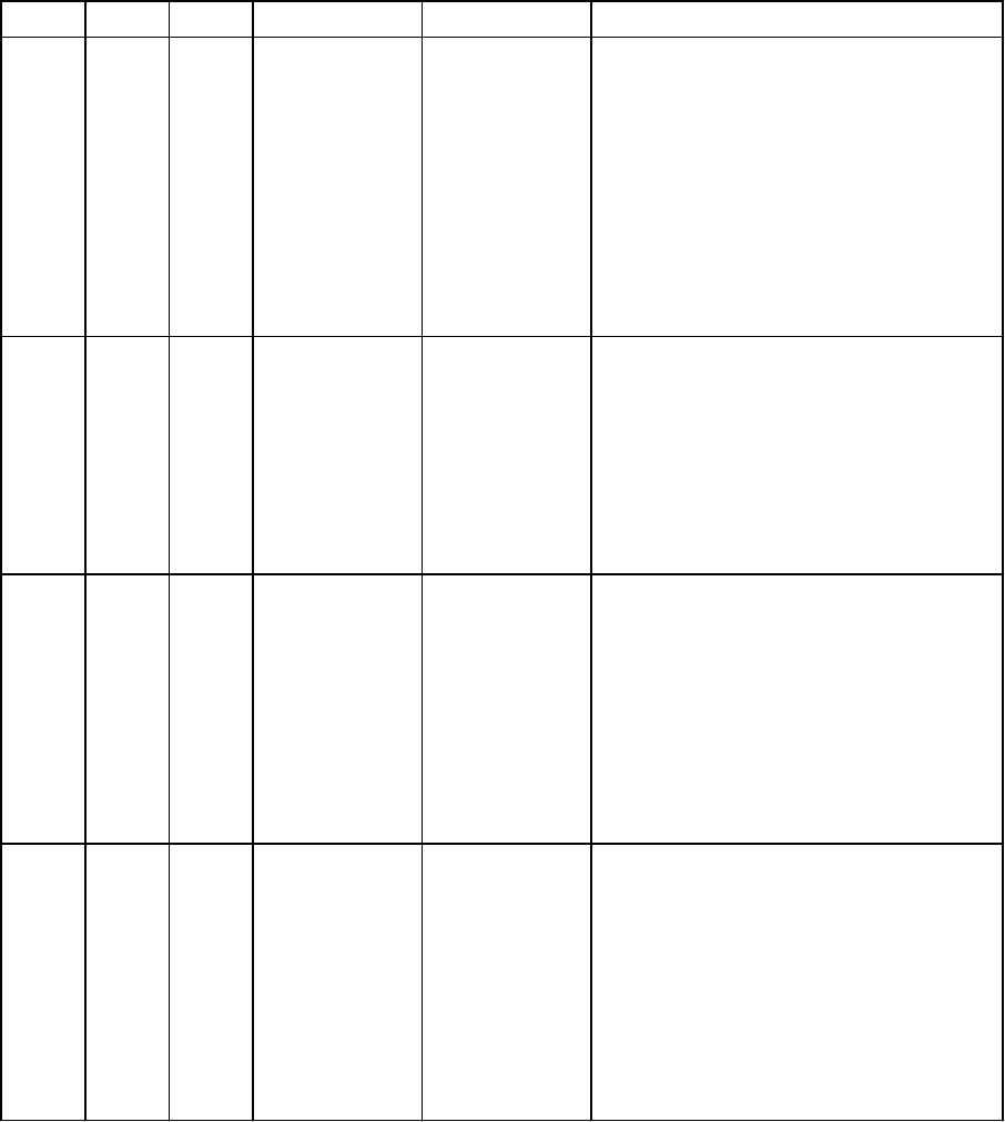
Table 1-3-5 Pin Function Summary (3/6)
Name No. I/O Function Other Function Description
SBO0A 18 Output P03, TXD0A
SBO0B 48 P70, TXD0B
SBO1A 15 P00, TXD1A
SBO1B 45 P73, TXD1B
SBO3 33 P51, SDA3
SBI0A 19 Input P04, RXD0A
SBI0B 49 P71, RXD0B
SBI1A 16 P01, RXD1A
SDA4A
SBI1B 46 P74, RXD1B
SBI3 32 P50
SBT0A 20 I/O P50
SBT0B 50 P72
SBT1A 17 P02, SCL4A
SBT1B 47 P75
SBT3 34 P52, SCL3
TXD0A 18 Output SBO0A, P03
TXD0B 48 SBO0B, P70
TXD1A 15 SBO1A, P00
TXD1B 45 SBO1B, P73
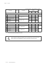
Transmission data output pins for serial
interfaces 0 , 1, 3. The output configuration,
either CMOS push-pull or n-channel open-drain
can be selected. Pull-up resistors can be
selected by the P0PLU register, the P5PLU
register and the P7PLUD register. Select output
mode by the P0DIR register, the P5DIR register
and the P7DIR register, and serial data output
mode by serial mode register 1 (SC0MD1,
SC1MD1, SC3MD1). These can be used as
normal I/O pins when the serial interface is not
used.
Reception data input pins for serial interfaces 0,
1, 3. Pll-up resistors can be selected by the
P0PLU register, the P5PLU register and the
P7PLUD register. Select input mode by the
P0DIR register, the P5DIR register, the P7DIR
register and serial input mode by the serial mode
register 1 ( SC0MD1, SC1MD1, SC3MD1). These
can be used as normal I/O pins when the serial
interface is not used.
Clock I/O pins for serial interfaces 0, 1,3. The
output configuration, either CMOS push-pull or n-
channel open-drain can be selected. Pull-up
resistors can be selected by the P0PLU resister
and the P5PLU register and the P7PLUD
register. Select clock I/O for each communication
mode by the P0DIR register, the P5DIR register,
the P7DIR register and serial mode register 1
( SC0MD1, SC1MD1, SC3MD1). These can be
used as normal I/O pins when the serial interface
is not used.
In the serial interface in UART mode, these pins
are configured as the transmission data output
pins. The output configuration, either CMOS
push-pull or n-channel open-drain can be
selected. Pull-up resistors can be selected by
the P0PLU register and the P7PLUD register.
Select output mode by the P0DIR register and the
P7DIR register, and serial data output by serial
interface 1 mode register 1 ( SC0MD1, SC1MD1).
These can be used as normal I/O pins when the
serial interface is not used.
Serial interface
transmission data
output pins
Serial interface
reception data input
pins
Serial interface
clock I/O pins
UART transmission
data output pins