


I - 11
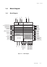
Chapter 1 Overview
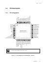
Pin Description
1-3-3 Pin Functions
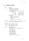
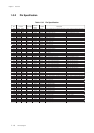
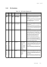
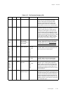
Table 1-3-3 Pin Function Summary (1/6)
Name No. I/O Function Other Function Description
VDD 7 Power supply pin
VSS 10
OSC1 9 Input Clock input pin
OSC2 8 Output Clock output pin
XI 11 Input Clock input pin
XO 12 Output Clock output pin
NRST 14 I/O Reset pin P27 This pin resets the chip when power is turned on,
is allocated as P27 and contains an internal pull-
up resistor. Setting this pin low initializes the
internal state of the device. Thereafter, setting the
input to high releases the reset. The hardware
waits for the system clock to stabilize, then
processes the reset interrupt. Also, if ""0"" is
written to P27 and the reset is initiated by
software, a low level will be output. The output
has an n-channel open-drain configuration. If a
capacitor is to be inserted between NRST and
VDD, it is recommended that a discharge diode
be placed between NRST and VDD.
P00 15 I/O I/O port 0 SBO1A, TXD1A
P01 16 SBI1A, RXD1A
SDA4B
P02 17 SBT1A, SCL4B
P03 18 SBO0A, TXD0A
P04 19 SBI0A, RXD0A
P05 20 SBT0A
P06 21 BUZZER
P10 22 I/O I/O port 1 TCO0A, RMOUTA
P11 23 TCIO0B, RMOUTB
P12 24 TCO4A
P13 25 TCIO4B
P14 26 TCI07
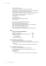
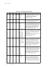
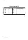
5-Bit CMOS tri-state I/O port.
Each bit can be set individually as either an input
or output by the P1DIR register. A pull-up resistor
for each bit can be selected individually by the
P1PLU register.
At reset, the input mode is selected and pull-up
resistors are disabled (high impedance output).
Supply 1.8 V to 3.6 V to VDD and 0 V to VSS.
Connect these oscillation pins to ceramic or
crystal oscillators for high-frequency clock
operation.
If the clock is an external input, connect it to OSC1
and leave OSC2 open. The chip will not operate
with an external clock when using either the
STOP or SLOW modes.
Connect these oscillation pins to ceramic
oscillators or crystal oscillators for low-frequency
clock operation.
If the clock is an external input, connect it to XI
and leave XO open. The chip will not operate with
an external clock when using the STOP mode. If
these pins are not used, connect XI to VSS and
leave XO open.
7-Bit CMOS tri-state I/O port.
Each bit can be set individually as either an input
or output by the P0DIR register. A pull-up resistor
for each bit can be selected individually by the
P0PLU register.
At reset, the input mode is selected and pull-up
resistors are disabled (high impedance output).