


Chapter 12 Serial Interface 3
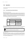
Operation
XII - 13
Forced Reset at Communication
It is possible to shut down the communication. A forced reset is operated by setting both of the
SC3SBOS flag and the SC3SBIS flag of the SC3MD1 register to "0" (the SBO3 pin function : port, input
data : input "1"). When a forced reset is operated, the SC3BSY flag of the SC3MD0 register, and the
IICBSY flag of the SC3CTR register are cleared, but other control registers hold their set values.
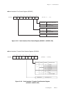
Last Bit of Transfer Data
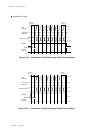
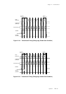
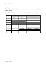
Table 12-3-4 shows the data output holding period of the last bit at transmission, and the minimum data
input period of the last bit at reception. At slave, setup for the internal clock is needed to keep data holding
time at data transmission. After the last bit data output holding period, "H" is output.
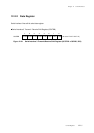
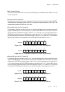
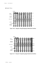
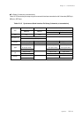
SC3CE1
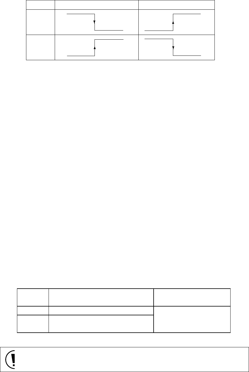
Received data input edge
Transmission data output edge
1
0
Table 12-3-3 Input Edge/Output Edge of Transmission/Received Data
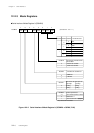
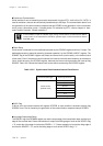
Data Input Pin Setup
There are 2 communication modes to be selected : 3 channels type (clock pin(SBT3 pin), data output pin
(SBO3 pin), data input pin (SBI3 pin)), 2 channels type (clock pin (SBT3 pin), data I/O pin (SBO3 pin)).
The SBI3 pin can be used only for serial data input. The SBO3 pin can be used for serial data input or
output. The SC3IOM flag of the SC3MD1 register can specify if serial data is input from the SBI3 pin, or
the SBO3 pin. When "data input from the SBO3 pin" is selected to communicate with 2 channels, the
SBO3 pin's direction control by the P5DIR3 flag of the P5DIR register can switch the transmission / recep-
tion. At that time, the SBI3 pin is not used, so that it can be used as a general port.
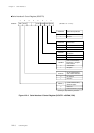
Table 12-3-4 Last Bit Data Length of Transmission Data
Transfer rate should be up to 2.5 MHz. If the transfer rate is over 2.5 MHz, the
transmission data cannot be output correctly.
at transmission at reception
the last bit data holding period the last bit data input period
at master 1 bit data length
[1 bit data length of external clock x 1/2]
+ [internal clock cycle x (1/2 to 3/2) ]
at slave
1 bit data length (minimum)