


Chapter 15 A/D Converter
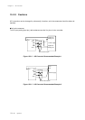
Operation
XV - 12
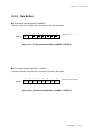
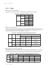
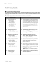
Setup Procedure
(1) Set the analog input pin.
PAIMD (x'3F3C')
bp0 : PAIMD0 = 1
PAPLUD (x'3F4A')
bp0 : PAPLUD0 = 0
PADIR (x'3F3A')
bp0 : PADIR0 = 0
(2) Select the analog input pin.
ANCTR1 (x'3FB1')
bp2-0 : ANCHS2-0 = 000
(3) Select the A/D converter clock.
ANCTR0 (x'3FB0')
bp5-4 : ANCK1-0 = 01
(4) Set the sample and hold time.
ANCTR0 (x'3FB0')
bp7-6 : ANSH1-0 = 01
(5) Set the interrupt level.
ADICR (x'3FFA')
bp7-6 : ADLV1-0 = 00
(6) Enable the interrupt.
ADICR (x'3FFA')
bp1 : ADIE = 1
Description
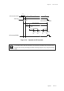
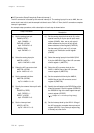
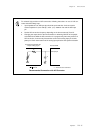
15-3-2 Setup Example
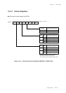
A/D Converter Setup Example by Registers
A/D conversion is started by setting registers. The analog input pins are set to AN0, the converter clock
is set to fs/4, and the sampling hold time is set to TAD x 6. Then, A/D conversion complete interrupt is
generated.
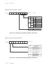
An example setup procedure, with a description of each step is shown below.
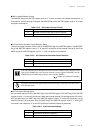
(1) Set the analog input pin (set at the procedure
2) to the special function pin by the port A input
mode register (PAIMD). Also, set to no pull-up/
pull-down resistance by the port A pull-up/pull-
down resistance control register (PAPLUD),
and to input mode by port A direction control
register (PADIR).
(2) Select the analog input pin from AN7-0 (PA7-
0) by the ANCHS2-0 flag of the A/D converter
control register 1 (ANCTR1).
(3) Select the A/D converter clock by the
ANCK1, ANCK0 flag of the A/D converter
control register 0 (ANCTR0).
(4) Set the sample and hold time by the ANSH1,
ANSH0 flag of the A/D converter control
register 0 (ANCTR0).
(5) Set the interrupt level by the ADLV1-0 flag of
the A/D conversion complete interrupt control
register (ADICR). If any interrupt request flag
is already set, clear them.
(6) Enable the interrupt by setting the ADIE flag
the ADICR register to "1".
[ Chapter 3. 3-1-4 Interrupt Flag Setting ]