


Chapter 11 Serial Interface 0, 1
XI - 58
Operation
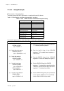
11-3-8 Setup Example
Transmission / Reception Setup
The setup example at UART transmission / reception with serial 0 is shown.
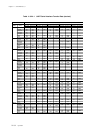
Table 11-3-33 shows the conditions at transmission / reception.
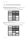
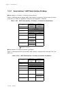
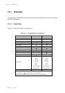
Table 11-3-33 UART Interface Transmision Reception Setup
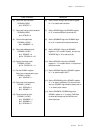
An example setup procedure, with a description of each step is shown below.
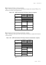
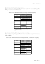
Setup Procedure Description
(1) Select prescaler operation.
PSCMD (x'3F6F')
bp0 : PSCEN = 1
(2) Select the clock source.
SC0CKS (x'3F97')
bp2-0 : SC0PSC2-0 = 110
(3) Select the used pin.
SC0ODC (x'3F96')
bp7 : SC0SEL = 0
(4) Control the pin type.
SC0ODC (x'3F96')
bp0 : SC0ODC0 = 1
P0PLU (x'3F40')
bp3 : P0PLU3 = 1
(5) Control the pin direction.
P0DIR (x'3F30')
bp4-3 : P0DIR4-3 = 01
(1) Set the PSCEN flag of the PSCMD register to
"1" to select prescaler operation.
(2) Set the bp2-0 flag of the SC0CKS
register to "110" to select timer 4 output as a
clock source.
(3) Set the SC0SEL flag of the SC0ODC
register to "0" to set I/O used pin to A (port 0).
(4) Set the SC0ODC0 flag of the SC0ODC
register to "1" to select N-ch open drain for the
TXD0A pin. Set the P0PLU3 flag of the P0PLU
register to "1" to add pull-up resistor.
(5) Set the P0DIR4-3 flag of the port 0 pin direction
control register (P0DIR) to "01" to set P03 to
output mode, and P04 to input mode.
Setup item set to
TXD / RXD pin independent (with 2 channels)
Frame mode specification 8 bits + 2 stop bits
First transfer bit MSB
Clock source timer 5
Used pin A (Port 0)
TXD0A / RX0DA pin type Nch open-drain
Pull-up resistor of TXD0A pin added
Parity bit add / check "0"add / check
Serial interface 0 transmission
complete interrupt
Enable.
Serial interface 0 reception
complete interrupt
Enable.